SA58603 データシートの表示(PDF) - Philips Electronics
部品番号
コンポーネント説明
メーカー
SA58603 Datasheet PDF : 15 Pages
| |||
Philips Semiconductors
High precision operational amplifier,
comparator, and voltage reference
Product data
SA58603
ORDERING INFORMATION
PACKAGE
TYPE NUMBER
NAME
DESCRIPTION
SA58603D
SO8
plastic small outline package; 8 leads; body width 3.9 mm
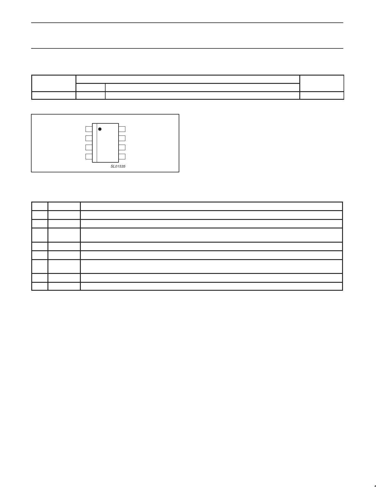
PIN CONFIGURATION
AIN+ 1
AIN– 2
AOUT 3
GND 4
TOP VIEW
SO8
8 VCC
7 COMPOUT
6 VS
5 COMIN–
SL01535
Figure 2. Pin configuration.
TEMPERATURE
RANGE
–40 to +85 °C
PIN DESCRIPTION
PIN SYMBOL
DESCRIPTION
1 AIN+
Non-inverting input of Op Amp. This is a PNP amplifier with the reference voltage as its supply voltage.
2 AIN–
Inverting input of Op Amp. This is a PNP amplifier with the reference voltage as its supply voltage.
3 AOUT
4 GND
Output of Op Amp. This is a NPN emitter follower output with a 22 kΩ internal on-chip pull-down resistor. Its supply
voltage is VCC.
Ground.
5 COMPIN– Inverting input of Comparator. This is a PNP amplifier with VCC as its positive supply voltage.
6 VS
Reference voltage output. The output reference is typically 1.27 V. The output reference is derived from the series
combination of a NPN transistor (configured as a diode with the base shorted to the collector) and a 120 kΩ resistor.
7 COMPOUT Output of Comparator. It is an open collector output stage which requires an external pull-up resistor.
8 VCC
Positive supply. Its operating range is 1.8 to 6.0 V.
2002 Nov 13
3
Share Link: 