PM6670S(2008) データシートの表示(PDF) - STMicroelectronics
部品番号
コンポーネント説明
メーカー
PM6670S Datasheet PDF : 53 Pages
| |||
PM6670S
Pin settings
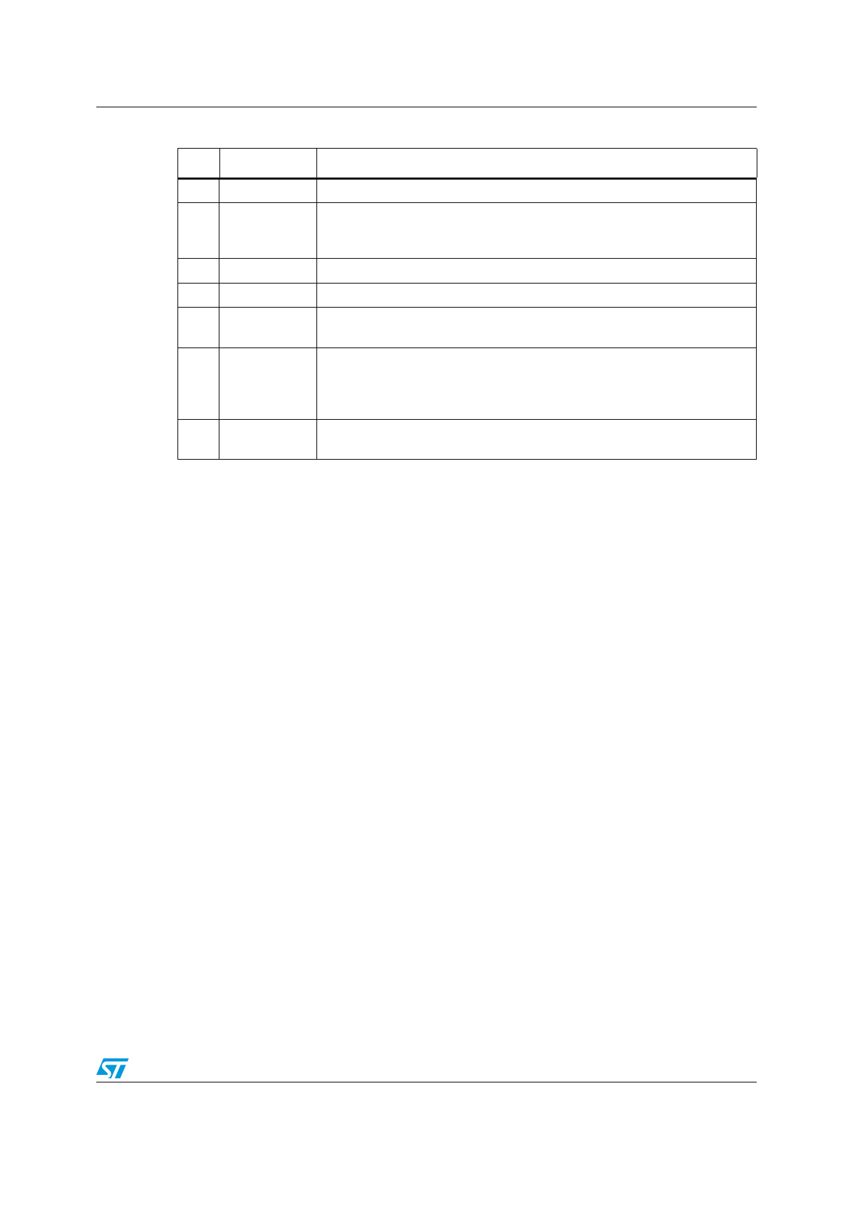
Table 2. Pin functions (continued)
N°
Pin
Function
18
VCC
+5 V Low-side gate driver supply. Bypass with a 100 nF capacitor to PGND.
Current Sense Input for the switching section. This pin must be connected
19
CSNS
through a resistor to the drain of the synchronous rectifier (RDSon sensing) to
set the current limit threshold.
20
PHASE Switch node connection and return path for the high-side gate driver.
21
HGATE High-side gate driver output
22
BOOT
Bootstrap capacitor connection. Positive Supply Input of the High-side Gate
Driver.
Linear regulator input. Connect to VDDQ in normal configuration or to a
23
LDOIN
lower supply to reduce the power dissipation. A 10 µF bypass ceramic
capacitor is suggested for noise rejection enhancement. See Section 7:
Device description on page 19
24
VTT
LDO linear regulator output. Bypass with a 20 µF (2x10 µF MLCC) filter
capacitor.
7/53
Share Link: 