74F219CW データシートの表示(PDF) - Fairchild Semiconductor
部品番号
コンポーネント説明
メーカー
74F219CW Datasheet PDF : 6 Pages
| |||
Unit Loading/Fan Out
Pin Names
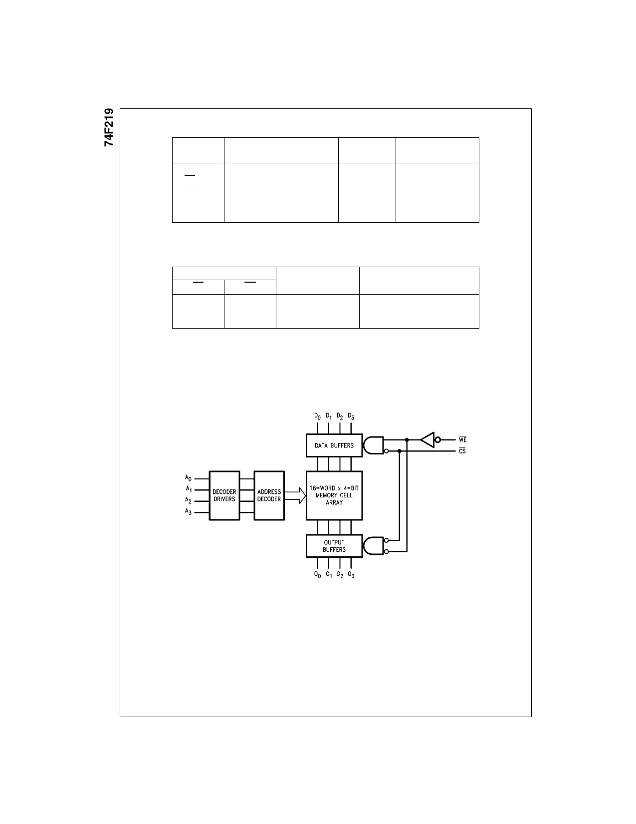
A0–A3
CS
WE
D0–D3
O0–O3
Description
Address Inputs
Chip Select Input (Active LOW)
Write Enable Input (Active LOW)
Data Inputs
3-STATE Data Outputs
U.L.
HIGH/LOW
1.0/1.0
1.0/2.0
1.0/1.0
1.0/1.0
150/40 (33.3)
Input IIH/IIL
Output IOH/IOL
20 µA/−0.6 mA
20 µA/−1.2 mA
20 µA/−0.6 mA
20 µA/−0.6 mA
−3 mA/24 mA (20 mA)
Function Table
Inputs
CS
WE
L
L
L
H
H
X
H = HIGH Voltage Level
L = LOW Voltage Level
X = Immaterial
Operation
Write
Read
Inhibit
Condition of Outputs
High Impedance
True Stored Data
High Impedance
Block Diagram
www.fairchildsemi.com
2
Share Link: 