MCM6729BWJ10 データシートの表示(PDF) - Motorola => Freescale
部品番号
コンポーネント説明
メーカー
MCM6729BWJ10 Datasheet PDF : 7 Pages
| |||
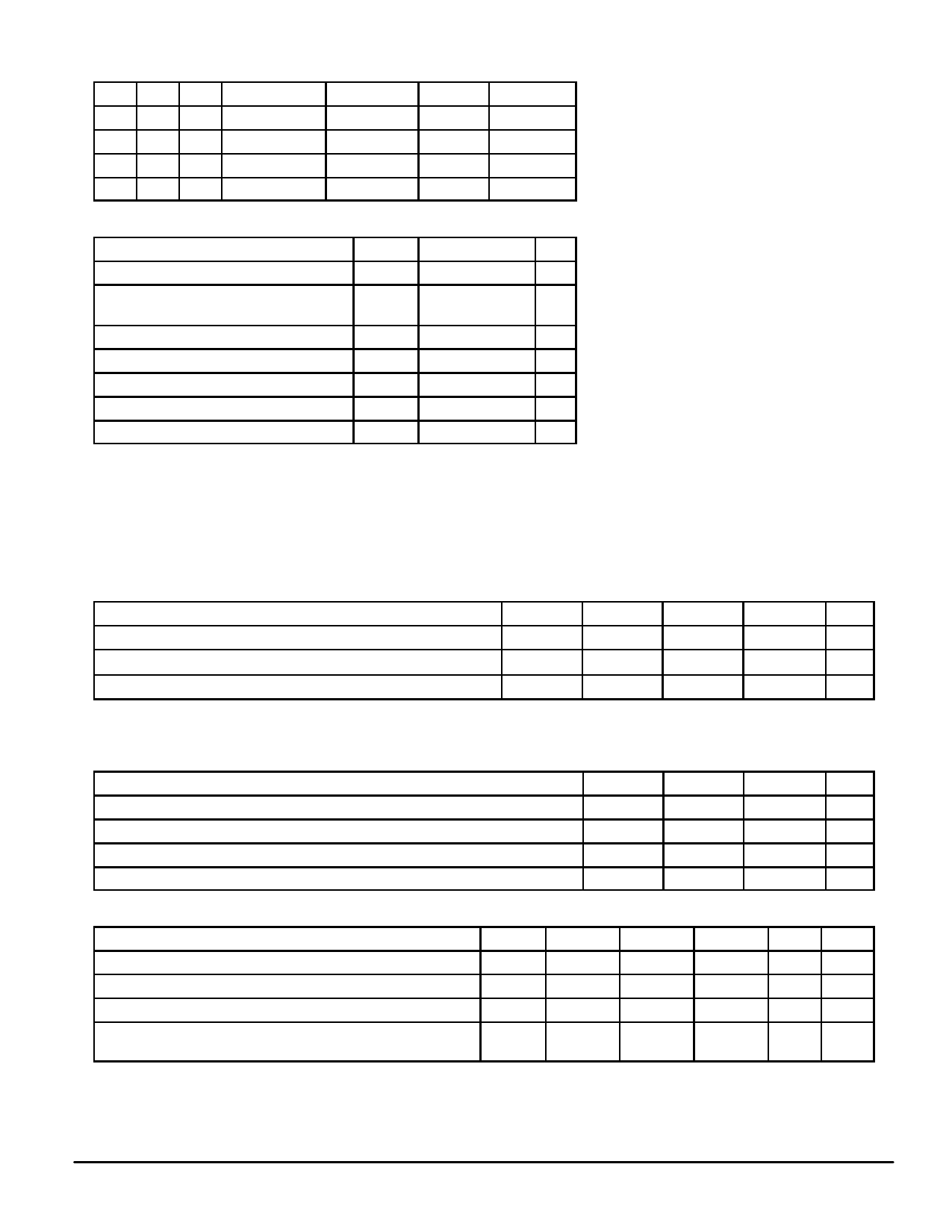
TRUTH TABLE (X = Don’t Care)
E
G
W
Mode
H
X
X
Not Selected
L
H
H Output Disabled
L
L
H
Read
L
X
L
Write
VCC Current
ISB1, ISB2
ICCA
ICCA
ICCA
Output
High–Z
High–Z
Dout
High–Z
Cycle
—
—
Read Cycle
Write Cycle
ABSOLUTE MAXIMUM RATINGS (See Note)
Rating
Symbol
Value
Unit
Power Supply Voltage
VCC
– 0.5 to + 7.0
V
Voltage Relative to VSS for Any Pin Except Vin, Vout – 0.5 to VCC + 0.5 V
VCC
Output Current
Iout
±30
mA
Power Dissipation
PD
1.2
W
Temperature Under Bias
Tbias
– 10 to + 85
°C
Operating Temperature
TA
0 to + 70
°C
Storage Temperature — Plastic
Tstg
– 55 to + 125
°C
NOTE: Permanent device damage may occur if ABSOLUTE MAXIMUM RATINGS are
exceeded. Functional operation should be restricted to RECOMMENDED OPER-
ATING CONDITIONS. Exposure to higher than recommended voltages for
extended periods of time could affect device reliability.
This device contains circuitry to protect the in-
puts against damage due to high static voltages
or electric fields; however, it is advised that nor-
mal precautions be taken to avoid application of
any voltage higher than maximum rated volt-
ages to these high–impedance circuits.
This BiCMOS memory circuit has been de-
signed to meet the dc and ac specifications
shown in the tables, after thermal equilibrium
has been established. The circuit is in a test
socket or mounted on a printed circuit board
and transverse air flow of at least 500 linear feet
per minute is maintained.
DC OPERATING CONDITIONS AND CHARACTERISTICS
(VCC = 5.0 V ± 10%, TA = 0 to 70°C, Unless Otherwise Noted)
RECOMMENDED OPERATING CONDITIONS
Parameter
Symbol
Min
Supply Voltage (Operating Voltage Range)
Input High Voltage
VCC
4.5
VIH
2.2
Input Low Voltage
VIL
– 0.5*
* VIL (min) = – 0.5 V dc; VIL (min) = – 2.0 V ac (pulse width ≤ 2.0 ns) for I ≤ 20.0 mA.
** VIH (max) = VCC + 0.3 V dc; VIH (max) = VCC + 2 V ac (pulse width ≤ 2.0 ns) for I ≤ 20.0 mA.
DC CHARACTERISTICS
Parameter
Input Leakage Current (All Inputs, Vin = 0 to VCC)
Output Leakage Current (E = VIH, Vout = 0 to VCC)
Output Low Voltage (IOL = + 8.0 mA)
Output High Voltage (IOH = – 4.0 mA)
Symbol
Ilkg(I)
Ilkg(O)
VOL
VOH
Typ
Max
Unit
5.0
5.5
V
—
VCC + 0.3** V
—
0.8
V
Min
Max
Unit
—
± 1.0
µA
—
± 1.0
µA
—
0.4
V
2.4
—
V
POWER SUPPLY CURRENTS
Parameter
Symbol 6729B–8 6729B–10 6729B–12 Unit
AC Active Supply Current (Iout = 0 mA) (VCC = max, f = fmax)
ICCA
195
165
155
mA
Active Quiescent Current (E = VIL, VCC = max, f = 0 MHz)
ICC2
90
90
90
mA
AC Standby Current (E = VIH, VCC = max, f = fmax)
ISB1
60
60
60
mA
CMOS Standby Current (VCC = max, f = 0 MHz, E ≥ VCC – 0.2 V,
ISB2
20
20
20
mA
Vin ≤ VSS + 0.2 V, or ≥ VCC – 0.2 V)
NOTES:
1. Reference AC Operating Conditions and Characteristics for input and timing (VIH/VIL, tr/tf, pulse level 0 to 3.0 V, VIH = 3.0 V).
2. All addresses transition simultaneously low (LSB) and then high (MSB).
3. Data states are all zero.
Notes
1, 2, 3
1, 2, 3
MCM6729B
2
MOTOROLA FAST SRAM
Share Link: 