MB15E05SRPV1 データシートの表示(PDF) - Fujitsu
部品番号
コンポーネント説明
メーカー
MB15E05SRPV1 Datasheet PDF : 25 Pages
| |||
MB15E05SR
s FUNCTIONAL DESCRIPTION
1. Pulse Swallow Function
The divide ratio can be calculated using the following equation:
fVCO = [(P × N) + A] × fOSC ÷ R (A < N)
fVCO : Output frequency of external voltage controlled oscillator (VCO)
N : Preset divide ratio of binary 11-bit programmable counter (3 to 2,047)
A : Preset divide ratio of binary 7-bit swallow counter (0 ≤ A ≤ 127)
fOSC : Output frequency of the reference frequency oscillator
R : Preset divide ratio of binary 14-bit programmable reference counter (3 to 16,383)
P : Preset divide ratio of modulus prescaler (64 or 128)
2. Serial Data Input
Serial data is processed using the Data, Clock, and LE pins. Serial data controls the programmable reference
divider and the programmable divider separately.
Binary serial data is entered through the Data pin.
One bit of data is shifted into the shift register on the rising edge of the Clock. When the LE signal pin is taken
high, stored data is latched according to the control bit data as follows:
Table 1. Control Bit
Control bit (CNT)
H
L
Destination of serial data
For the programmable reference divider
For the programmable divider
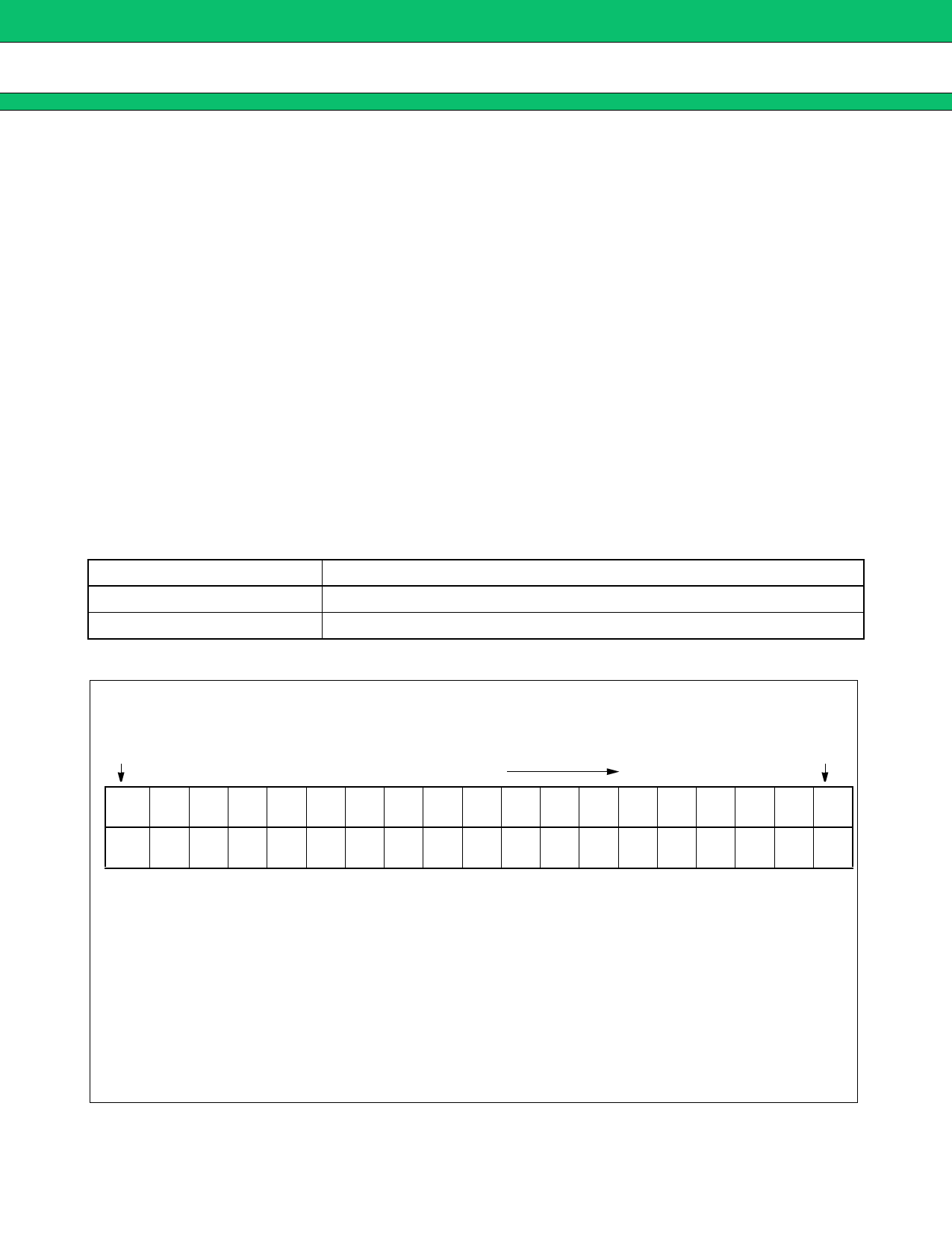
(1) Shift Register Configuration
Programmable Reference Counter
LSB
Data Flow
MSB
1 2 3 4 5 6 7 8 9 10 11 12 13 14 15 16 17 18 19
CNT R1 R2 R3 R4 R5 R6 R7 R8 R9 R10 R11 R12 R13 R14 SW FC LDS CS
CNT
R1 to R14
SW
FC
LDS
CS
: Control bit
[Table 1]
: Divide ratio setting bit for the programmable reference counter (3 to 16,383) [Table 2]
: Divide ratio setting bit for the prescaler (64/65 or 128/129)
[Table 5]
: Phase control bit for the phase comparator
[Table 8]
: LD/fOUT signal select bit
[Table 7]
: Charge pump current select bit
[Table 6]
Note: Start data input with MSB first.
8
Share Link: 