MAX15035ETL データシートの表示(PDF) - Maxim Integrated
部品番号
コンポーネント説明
メーカー
MAX15035ETL Datasheet PDF : 28 Pages
| |||
MAX15035
15A Step-Down Regulator with Internal Switches
Electrical Characteristics 2 (continued)
(Circuit of Figure 1, VIN = 12V, VDD = VCC = VEN = 5V, REFIN = ILIM = REF, SKIP = GND. TA = -40°C to +85°C, unless otherwise
specified.) (Note 1)
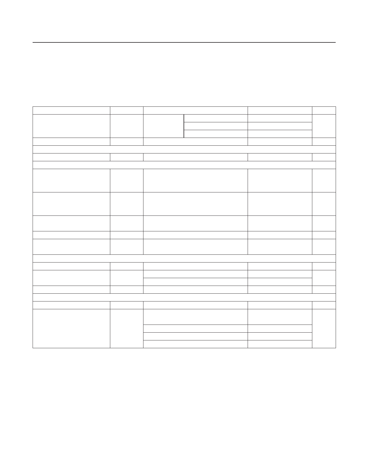
FB Voltage Range
FB Voltage Accuracy
PARAMETER
REFERENCE
Reference Voltage
FAULT DETECTION
Output Overvoltage-Protection
Trip Threshold
VFB
VFB
SYMBOL
(Note 2)
Measured at FB, VREFIN = 0.5V
VIN = 4.5V to
VREFIN = 1.0V
26V, SKIP = VDD VREFIN = 2.0V
CONDITIONS
VREF
VDD = 4.5V to 5.5V
OVP
With respect to the internal target voltage
(error comparator threshold) rising edge;
hysteresis = 50mV
0
0.49
0.99
1.985
MIN
1.985
250
VREF
0.51
1.01
2.015
MAX
V
V
UNITS
2.015
V
350
mV
Output Undervoltage-Protection
Trip Threshold
UVP
With respect to the internal target voltage
(error comparator threshold);
falling edge; hysteresis = 50mV
-240
-160
mV
Output Undervoltage
Fault-Propagation Delay
PGOOD Output-Low Voltage
VCC Undervoltage Lockout
Threshold
CURRENT LIMIT
ILIM Input Range
Current-Limit Threshold
Ultrasonic Frequency
INPUTS AND OUTPUTS
EN Logic-Input Threshold
SKIP Quad-Level Input
Logic Levels
tUVP
FB forced 25mV below trip threshold
ISINK = 3mA
VUVLO(VCC)
Rising edge, PWM disabled below this level,
hysteresis = 100mV
80
3.95
0.4
VILIMIT
VILIM = 0.4V, VGND = VLX
ILIM = REF (2.0V), VGND - VLX
17
90
SKIP = open (3.3V), VFB = VREFIN + 50mV
17
VEN
V SKIP
EN rising edge hysteresis = 450mV (typ)
High (5V VDD)
Mid (3.3V)
Ref (2.0V)
Low (GND)
1.20
VCC -
0.4
3.0
1.7
400
µs
0.4
V
4.45
V
VREF
V
23
mV
110
kHz
2.20
V
3.6
V
2.3
0.4
Note 1: Limits are 100% production tested at TA = +25°C. Maximum and minimum limits over temperature are guaranteed by
design and characterization.
Note 2: The 0 to 0.5V range is guaranteed by design, not production tested.
Note 3: On-time and off-time specifications are measured from 50% point to 50% point at the unloaded LX node. The typical 25ns
dead time that occurs between the high-side driver falling edge (high-side MOSFET turn-off) and the low-side MOSFET
turnon) is included in the on-time measurement. Similarly, the typical 25ns dead time that occurs between the low-side
driver falling edge (low-side MOSFET turn-off) and the high-side driver rising edge (high-side MOSFET turn-on) is included
in the off-time measurement.
www.maximintegrated.com
Maxim Integrated │ 5
Share Link: 