LT3015 データシートの表示(PDF) - Linear Technology
部品番号
コンポーネント説明
メーカー
LT3015 Datasheet PDF : 26 Pages
| |||
LT3015 Series
APPLICATIONS INFORMATION
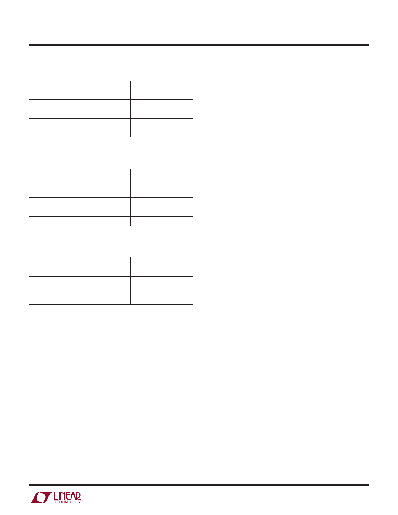
Table 2. Measured Thermal Resistance for DFN Package
COPPER AREA
TOP SIDE* BACKSIDE
BOARD THERMAL RESISTANCE
AREA (JUNCTION-TO-AMBIENT)
2500mm2 2500mm2 2500mm2
40°C/W
1000mm2
225mm2
2500mm2
2500mm2
2500mm2
2500mm2
40°C/W
41°C/W
100mm2 2500mm2 2500mm2
42°C/W
*Device is mounted on topside
Table 3. Measured Thermal Resistance for MSOP Package
COPPER AREA
TOP SIDE*
2500mm2
BACKSIDE
2500mm2
BOARD
AREA
2500mm2
THERMAL RESISTANCE
(JUNCTION-TO-AMBIENT)
37°C/W
1000mm2 2500mm2 2500mm2
37°C/W
225mm2 2500mm2 2500mm2
38°C/W
100mm2 2500mm2 2500mm2
40°C/W
*Device is mounted on topside
Table 4. Measured Thermal Resistance for DD-Pak Package
COPPER AREA
TOP SIDE*
2500mm2
1000mm2
225mm2
BACKSIDE
2500mm2
2500mm2
2500mm2
BOARD
AREA
2500mm2
2500mm2
2500mm2
THERMAL RESISTANCE
(JUNCTION-TO-AMBIENT)
14°C/W
16°C/W
19°C/W
*Device is mounted on topside
T Package, 5-Lead TO-220
Thermal Resistance (Junction-to-Case) = 3°C/W
Calculating Junction Temperature
Example: Given an output voltage of –2.5V, an input voltage
range of –3.3V ± 5%, an output current range of 1mA to
500mA, and a maximum ambient temperature of 85°C,
what is the maximum junction temperature?
The power dissipated by the LT3015 equals:
IOUT(MAX) • (VIN(MAX) - VOUT) + IGND • (VIN(MAX))
where:
IOUT(MAX) = –500mA
VIN(MAX) = –3.465V
IGND at (IOUT = –500mA, VIN = –3.465V) = –6.5mA
Thus:
P = –500mA(–3.465V + 2.5V) + –6.5mA • (–3.465V) =
0.505W
Using a DFN package, the thermal resistance is in the
range of 40°C/W to 42°C/W depending on the copper area.
Therefore, the junction temperature rise above ambient
approximately equals:
0.505W • 41°C/W = 20.7°C
The maximum junction temperature equals the maxi-
mum ambient temperature plus the maximum junction
temperature rise above ambient or:
TJMAX = 85°C + 20.7°C = 105.7°C
Protection Features
The LT3015 incorporates several protection features that
make it ideal for use in battery-powered applications. In
addition to the normal protection features associated
with monolithic regulators, such as current limiting and
thermal limiting, the device protects itself against reverse
input voltages and reverse output voltages.
Precision current limit and thermal overload protections
are intended to protect the LT3015 against current over-
load conditions at the output of the device. For normal
operation, do not allow the the junction temperature to
exceed 125°C.
Pulling the LT3015’s output above ground induces no
damage to the part. If IN is left open circuit or grounded,
OUT can be pulled above GND by 30V. In addition, OUT acts
like an open circuit, i.e. no current flows into the pin. If IN
is powered by a voltage source, OUT sinks the LT3105’s
short-circuit current and protects itself by thermal limiting.
In this case, grounding the SHDN pin turns off the device
and stops OUT from sinking the short-circuit current.
3015fb
19
Share Link: 