LH28F320BFE-PTTL60 データシートの表示(PDF) - Sharp Electronics
部品番号
コンポーネント説明
メーカー
LH28F320BFE-PTTL60 Datasheet PDF : 37 Pages
| |||
LHF32FB1
9
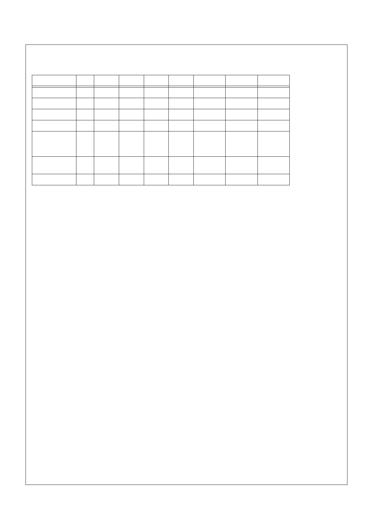
Table 5. Bus Operation(1, 2)
Mode
Notes RST# CE# OE# WE# Address DQ0-15 RY/BY# (8)
Read Array
6
VIH
VIL
VIL
VIH
X
DOUT
X
Output Disable
VIH
VIL
VIH
VIH
X
High Z
X
Standby
VIH
VIH
X
X
X
High Z
X
Reset
3
VIL
X
X
X
X
High Z High Z
Read Identifier
Codes/OTP
6
VIH
VIL
VIL
See
See
VIH Table 3 and Table 3 and
Table 4 Table 4
X
Read Query
6,7 VIH
VIL
VIL
VIH
See
See
Appendix Appendix
X
Write
4,5,6 VIH
VIL
VIH
VIL
X
DIN
X
NOTES:
1. See DC Characteristics for VIL or VIH voltages.
2. X can be VIL or VIH.
3. RST# at GND±0.2V ensures the lowest power consumption.
4. Command writes involving block erase, full chip erase, (page buffer) program or OTP program are reliably
executed when VCC=2.7V-3.6V.
5. Refer to Table 6 for valid DIN during a write operation.
6. Never hold OE# low and WE# low at the same timing.
7. Refer to Appendix of LH28F320BF series for more information about query code.
8. RY/BY# is VOL when the WSM (Write State Machine) is executing internal block erase, full chip erase,
(page buffer) program or OTP program algorithms. It is High Z during when the WSM is not busy, in
block erase suspend mode (with program and page buffer program inactive), (page buffer) program suspend
mode, or reset mode.
Rev. 2.44
Share Link: 