KA3016D データシートの表示(PDF) - Fairchild Semiconductor
部品番号
コンポーネント説明
メーカー
KA3016D Datasheet PDF : 18 Pages
| |||
KA3016D
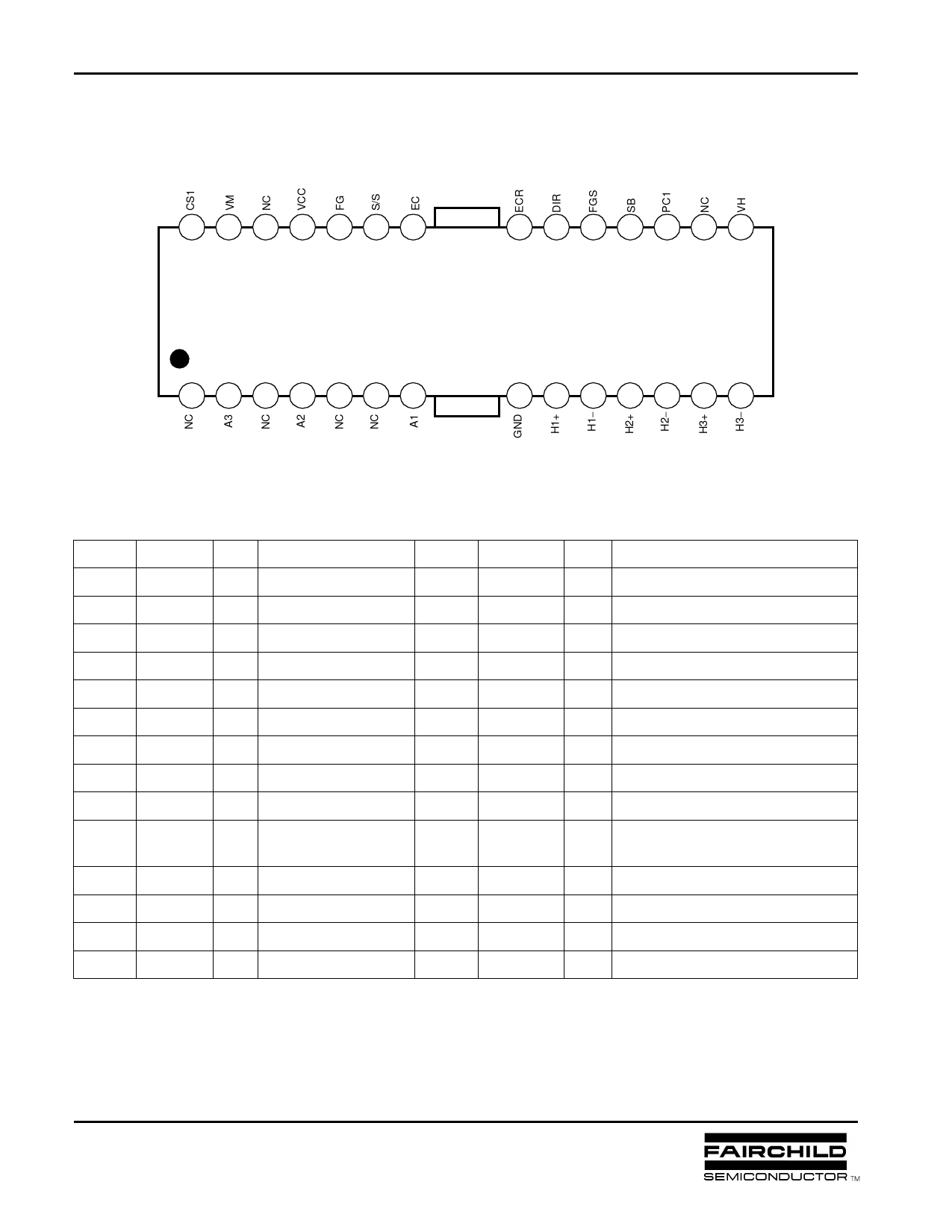
PIN CONFIGURATION
CD-ROM PRODUCTS
FIN(GND)
28 27 26 25 24 23 22
21 20 19 18 17 16 15
KA3016D
1
2
3
4
5
6
7
8
9 10 11 12 13 14
FIN(GND)
PIN DESCRIPTIONS
Pin No. Symbol
1
NC
2
A3
3
NC
4
A2
5
NC
6
NC
7
A1
8
GND
9
H1+
10
H1−
I/O
Description
− No connection
O Output (A3)
− No connection
O Output (A2)
− No connection
− No connection
O Output (A1)
− Ground
I Hall signal (H1+)
I Hall signal (H1−)
11
H2+
I Hall signal (H2+)
12
H2−
I Hall signal (H2−)
13
H3+
I Hall signal (H3+)
14
H3−
I Hall signal (H3−)
Pin No. Symbol
15
VH
16
NC
17
PC1
18
SB
19
FGS
20
DIR
21
ECR
22
EC
23
S/S
24
FG
25
VCC
26
NC
27
VM
28
CS1
I/O
Description
I Hall bias
− No connection
− Phase compensation capacitor
I Short brake
I Frequency generation selection
O Rotational direction output
I Output current control reference
I Output current control voltage
I Power save (Start/Stop switch)
O Frequency generation waveform
(3X or 1X hall frequency)
− Supply voltage (Signal)
− No connection
− Supply voltage (Motor)
− Output current detection
2
MIC-99D001
January 1999
Share Link: 