FAN48630BUC34X データシートの表示(PDF) - Fairchild Semiconductor
部品番号
コンポーネント説明
メーカー
FAN48630BUC34X
Fairchild Semiconductor
FAN48630BUC34X Datasheet PDF : 15 Pages
| |||
Application Information
Output Capacitance (COUT)
Stability
The effective capacitance (CEFF) of small, high-value, ceramic
capacitors decreases as bias voltage increases.
FAN48630 is guaranteed for stable operation with the
minimum value of CEFF (CEFF(MIN)) outlined in Table 4 below.
Table 4. Minimum CEFF Required for Stability
Operating Conditions
VOUT (V)
3.15
ILOAD (mA)
0 to 1500
CEFF(MIN)
(F)
12
3.5
0 to 1500
9
4.5 and 5
0 to 1500
6
CEFF varies with manufacturer, material, and case size.
Inductor Selection
Recommended nominal inductance value is 0.47 H.
FAN48630 employs valley-current limiting; peak inductor
current can reach 3.8 A for a short duration during overload
conditions. Saturation effects cause the inductor current ripple
to become higher under high loading as only valley of the
inductor current ripple is controlled.
For FAN48630UC315X and FAN48630UC33X, a 0.33 H
inductor can be used for improved transient performance.
Startup
Input current limiting is in effect during soft-start, which limits
the current available to charge COUT and any additional
capacitance on the VOUT line. If the output fails to achieve
regulation within the limits described in the Startup section, a
FAULT occurs, causing the circuit to shut down then restart
after a significant time period. If the total combined output
capacitance is very high, the circuit may not start on the first
attempt, but eventually achieves regulation if no load is
present. If a high-current load and high capacitance are both
present during soft-start, the circuit may fail to achieve
regulation and continually attempts soft-start, only to have
the output capacitance discharged by the load when in a
FAULT state.
Output Voltage Ripple
Output voltage ripple is inversely proportional to COUT. During
tON, when the boost switch is on, all load current is supplied by
COUT. Output ripple is calculated as:
VRIPPLE (PP)
tON
I LOAD
COUT
and
EQ. 3
tON
tSW
D
tSW
1
VIN
VOUT
therefore:
EQ. 4
VRIPPLE (P P)
tSW
1
VIN
VOUT
I LOAD
COUT
and
EQ. 5
tSW
1
fSW
EQ. 6
As can be seen from EQ. 5, the maximum VRIPPLE occurs
when VIN is at minimum and ILOAD is at maximum.
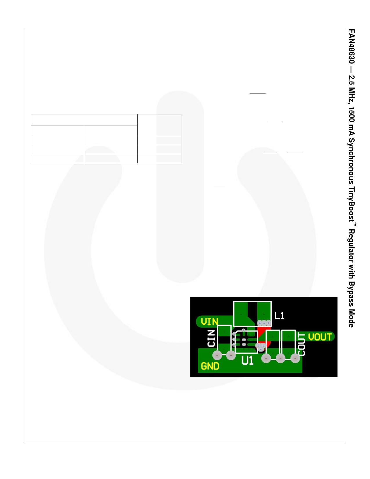
Layout Recommendations
The layout recommendations below highlight various top-
copper pours using different colors.
To minimize spikes at VOUT, COUT must be placed as close as
possible to PGND and VOUT, as shown in Figure 29.
For thermal reasons, it is suggested to maximize the pour
area for all planes other than SW. Especially the ground pour
should be set to fill all available PCB surface area and tied to
internal layers with a cluster of thermal vias.
Figure 29. Layout Recommendation
© 2011 Fairchild Semiconductor Corporation
FAN48630 • Rev. 1.0.5
13
www.fairchildsemi.com
Share Link: 