AD7656BSTZ-1-RL データシートの表示(PDF) - Analog Devices
部品番号
コンポーネント説明
メーカー
AD7656BSTZ-1-RL
Analog Devices
AD7656BSTZ-1-RL Datasheet PDF : 32 Pages
| |||
AD7656-1/AD7657-1/AD7658-1
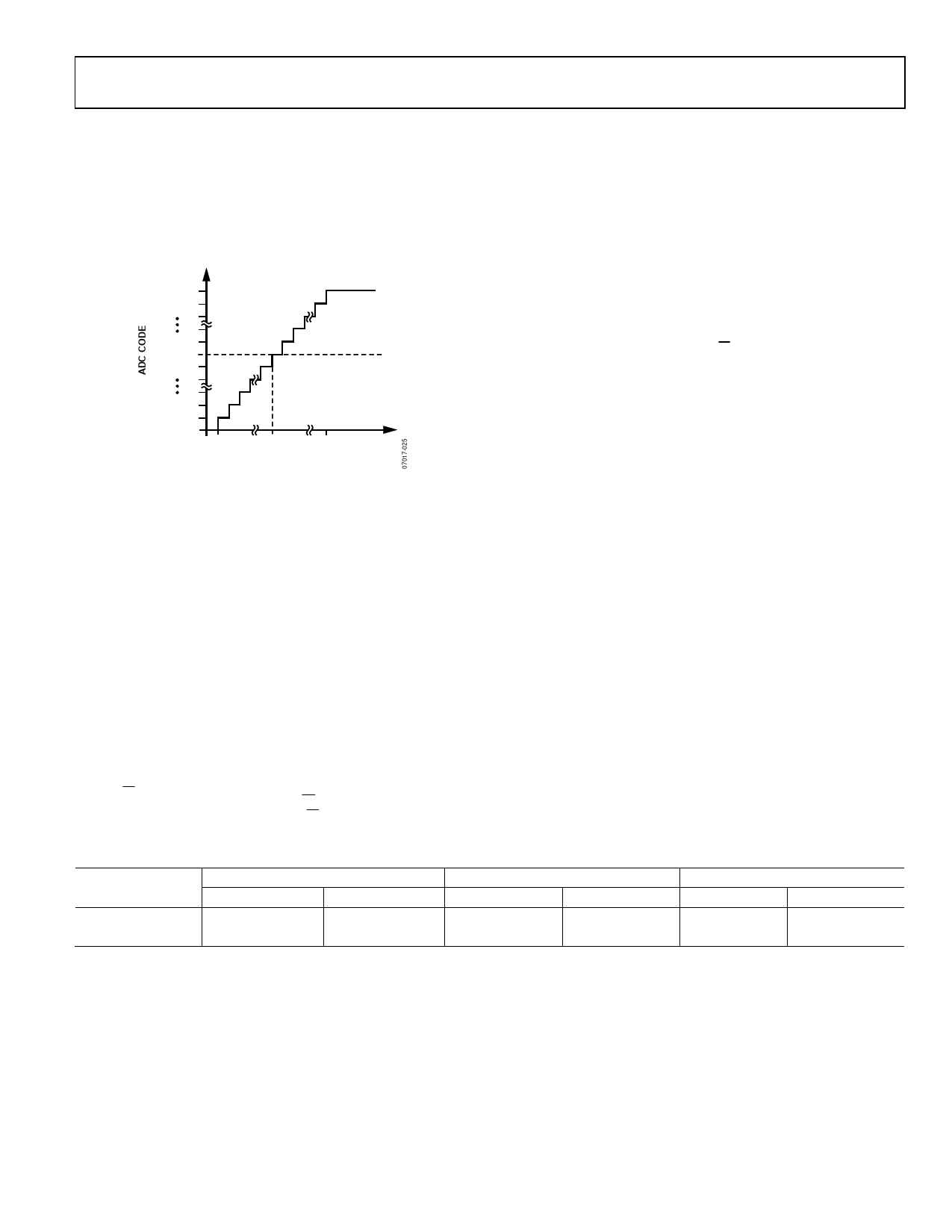
ADC TRANSFER FUNCTION
The output coding of the AD7656-1/AD7657-1/AD7658-1 is
twos complement. The designed code transitions occur midway
between successive integer LSB values, that is, 1/2 LSB, 3/2 LSB.
The LSB size is FSR/65,536 for the AD7656-1, FSR/16,384 for
the AD7657-1, and FSR/4096 for the AD7658-1. The ideal
transfer characteristic is shown in Figure 26.
011 ... 111
011 ... 110
000 ... 001
000 ... 000
111 ... 111
100 ... 010
100 ... 001
100 ... 000
–FSR/2 + 1/2LSB
AGND – 1LSB +FSR/2 – 3/2LSB
ANALOG INPUT
Figure 26. AD7656-1/AD7657-1/AD7658-1 Transfer Characteristic
The LSB size is dependent on the analog input range selected
(see Table 9).
INTERNAL/EXTERNAL REFERENCE
The REFIN/REFOUT pin allows access to the 2.5 V reference of
the AD7656-1/AD7657-1/AD7658-1, or it allows an external
reference to be connected to provide the reference source for
conversions.
The AD7656-1/AD7657-1/AD7658-1 can each accommodate a
2.5 V external reference range. When using an external reference,
the internal reference must be disabled. After a reset, the AD7656-1/
AD7657-1/AD7658-1 default to operating in external reference
mode with the internal reference buffers enabled.
The internal reference can be enabled in either hardware or
software mode. To enable the internal reference in hardware mode,
set the H/S SEL pin to 0 and the REFEN/DIS pin to 1. To enable the
internal reference in software mode, set H/S SEL to 1 and write to
the control register to set DB9 of the register to 1. For the internal
reference mode, the REFIN/REFOUT pin should be decoupled
using a 1 μF capacitor.
The AD7656-1/AD7657-1/AD7658-1 each contain three on-
chip reference buffers. Each of the three ADC pairs has an
associated reference buffer. These reference buffers require
external decoupling capacitors, using 1 μF capacitors, on the
REFCAPA, REFCAPB, and REFCAPC pins. The internal
reference buffers can be disabled in software mode by writing
to Bit DB8 in the internal control register. If serial interface is
selected, the internal reference buffers can be disabled in hardware
mode by setting the DB14/REFBUFEN/DIS pin high. If the internal
reference and its buffers are disabled, an external buffered
reference should be applied to the REFCAPx pins.
TYPICAL CONNECTION DIAGRAM
Figure 27 shows the typical connection diagram for the AD7656-1/
AD7657-1/AD7658-1, illustrating the reduction in the number
and value of decoupling capacitors required. There are eight
AVCC supply pins on each part. The AVCC supplies are the supplies
used for the AD7656-1/AD7657-1/AD7658-1 conversion process;
therefore, they should be well decoupled. The AVCC supply which
is applied to eight AVCC pins can be decoupled using just one 1 μF
capacitor The AD7656-1/AD7657-1/AD7658-1 can operate with
the internal reference or an externally applied reference. In this
configuration, the parts are configured to operate with the
external reference. The REFIN/REFOUT pin is decoupled with
a 1 μF capacitor. The three internal reference buffers are enabled.
Each of the REFCAPx pins is decoupled with a 1 μF capacitor.
If the same supply is being used for the AVCC and DVCC supplies, a
ferrite or small RC filter should be placed between the supply pins.
AGND pins are connected to the AGND plane of the system.
The DGND pins are connected to the digital ground plane in
the system. The AGND and DGND planes should be connected
together at one place in the system. This connection should be
as close as possible to the AD7656-1/AD7657-1/AD7658-1 in
the system.
Table 9. LSB Size for Each Analog Input Range
Input Range for AD7656-1
Parameter
±10 V
±5 V
LSB Size
0.305 mV
0.152 mV
FS Range
20 V/65,536
10 V/65,536
Input Range for AD7657-1
±10 V
±5 V
1.22 mV
0.610 mV
20 V/16,384
10 V/16,384
Input Range for AD7658-1
±10 V
±5 V
4.88 mV
2.44 mV
20 V/4096
10 V/4096
Rev. 0 | Page 21 of 32
Share Link: 