ADSP-21266 データシートの表示(PDF) - Analog Devices
部品番号
コンポーネント説明
メーカー
ADSP-21266 Datasheet PDF : 48 Pages
| |||
ADSP-21261/ADSP-21262/ADSP-21266
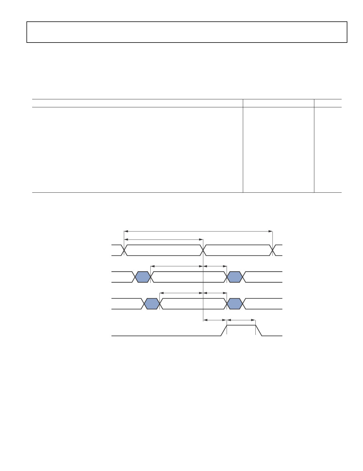
Parallel Data Acquisition Port (PDAP)
The timing requirements for the PDAP are provided in Table 34
and Figure 24. PDAP is the parallel mode operation of
Channel 0 of the IDP. For details on the operation of the IDP,
see the IDP chapter of the ADSP-2126x Peripherals Manual.
Note that the most significant 16 bits of external PDAP data can
be provided through either the parallel port AD15–0 or the
DAI_P20–5 pins. The remaining four bits can only be sourced
through DAI_P4–1. The timing below is valid at the
DAI_P20–1 pins or at the AD15–0 pins.
Table 34. Parallel Data Acquisition Port (PDAP)
Parameter
Timing Requirements
tSPHOLD
tHPHOLD
tPDSD
tPDHD
PDAP_HOLD Setup Before PDAP_CLK Sample Edge1
PDAP_HOLD Hold After PDAP_CLK Sample Edge1
PDAP_DAT Setup Before SCLK PDAP_CLK Sample Edge1
PDAP_DAT Hold After SCLK PDAP_CLK Sample Edge1
tPDCLKW
Clock Width
tPDCLK
Clock Period
Min
Max
Unit
2.5
ns
2.5
ns
2.5
ns
2.5
ns
7
ns
20
ns
Switching Characteristics
tPDHLDD
Delay of PDAP Strobe After Last PDAP_CLK Capture Edge for a Word
2 × tCCLK
ns
tPDSTRB
PDAP Strobe Pulse Width
1 × tCCLK – 1
ns
1 Source pins of DATA are ADDR7–0, DATA7–0, or DAI pins. Source pins for SCLK and FS are: 1) DAI pins, 2) CLKIN through PCG, or 3) DAI pins through PCG.
DAI_P20–1
(PDAP_CLK)
DAI_P20–1
(PDAP_HOLD)
DAI_P20–1/
ADDR23–4
(PDAP_DATA)
DAI_P20–1
(PDAP_STROBE)
SAMPLE EDGE
tPDCLKW
tPDCLK
tSPHOLD
tHPHOLD
tPDSD
tPDHD
tPDHLDD
tPDSTRB
Figure 24. Parallel Data Acquisition Port (PDAP)
Rev. G | Page 33 of 48 | December 2012
Share Link: 