ADP3121(2009) データシートの表示(PDF) - ON Semiconductor
部品番号
コンポーネント説明
メーカー
ADP3121 Datasheet PDF : 10 Pages
| |||
ADP3121
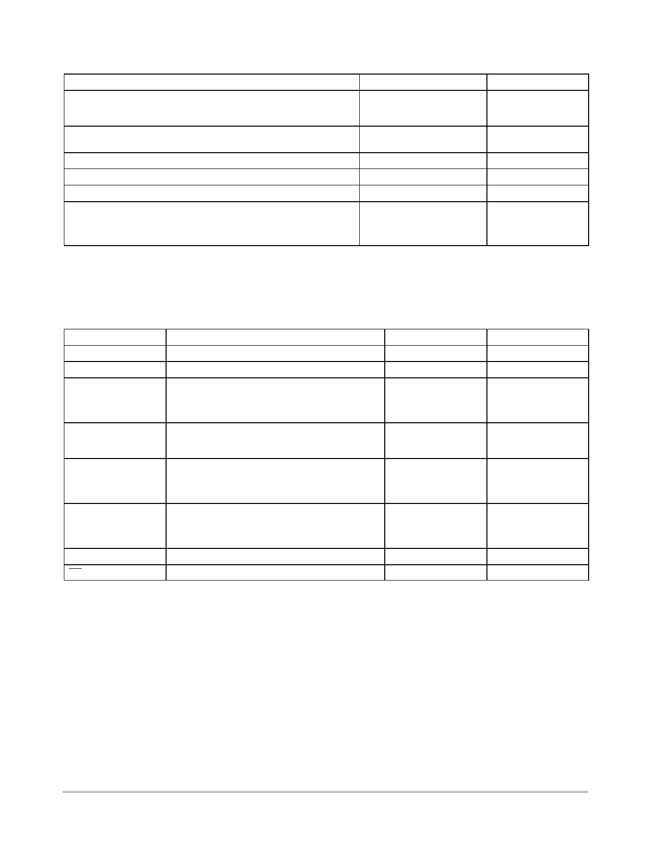
MAXIMUM RATINGS
Rating
Value
Unit
qJA, SOIC_N
2−Layer Board
123
°C/W
4−Layer Board
90
°C/W
qJA, LFCSP_VD (Note 1)
4−Layer Board
64.3
°C/W
Operating Ambient Temperature Range
0 to 85
°C
Junction Temperature Range
0 to 150
°C
Storage Temperature Range
−65 to +150
°C
Lead Temperature
Soldering (10 sec)
300
°C
Vapor Phase (60 sec)
215
°C
Infrared (15 sec)
260
°C
Stresses exceeding Maximum Ratings may damage the device. Maximum Ratings are stress ratings only. Functional operation above the
Recommended Operating Conditions is not implied. Extended exposure to stresses above the Recommended Operating Conditions may affect
device reliability.
1. Internally limited by thermal shutdown, 150°C min.
2. 2 layer board, 1 in2 Cu, 1 oz thickness.
3. 60−180 seconds minimum above 237°C.
4. This device is ESD sensitive. Use standard ESD precautions when handling
ABSOLUTE MAXIMUM RATINGS
Pin Symbol
Pin Name
VCC
GND
Main supply voltage input
Ground
BST
Bootstrap Supply Voltage Input
DC
<200 ns
BST to SW
SW
Switching Node
(Bootstrap Supply Return)
DC
<200 ns
DRVH
High−Side Driver Output
DC
<20 ns
<200 ns
DRVL
Low−Side Driver Output
DC
<20 ns
<200 ns
IN
DRVH and DRVL Control Input
OD
Outside Disable
Vmax
15 V
0V
VCC + 15
+35
+15
+15
+25 V
BST + 0.3
BST + 2 V
BST + 0.3 V
VCC + 0.3 V
VCC + 2 V
VCC + 0.3 V
6.5 V
6.5 V
Vmin
−0.3 V
0V
−0.3 V
−0.3 V
−0.3 V
−5 V
−10 V
SW − 0.3 V
SW − 2 V
SW − 2 V
−0.3 V
−2 V
−2 V
−0.3 V
−0.3 V
NOTE: All voltages are with respect to PGND except where noted.
Stresses exceeding Maximum Ratings may damage the device. Maximum Ratings are stress ratings only. Functional operation above the
Recommended Operating Conditions is not implied. Extended exposure to stresses above the Recommended Operating Conditions may affect
device reliability.
http://onsemi.com
3
Share Link: 