AD8200YCHIPS データシートの表示(PDF) - Analog Devices
部品番号
コンポーネント説明
メーカー
AD8200YCHIPS Datasheet PDF : 12 Pages
| |||
AD8200
CURRENT SENSING
High Line, High Current Sensing
Basic automotive applications making use of the large common-
mode range are shown in Figures 1 and 2. The capability of the
device to operate as an amplifier in primary battery supply circuits
is shown in Figure 1; Figure 2 illustrates the ability of the device
to withstand voltages below system ground.
Low Current Sensing
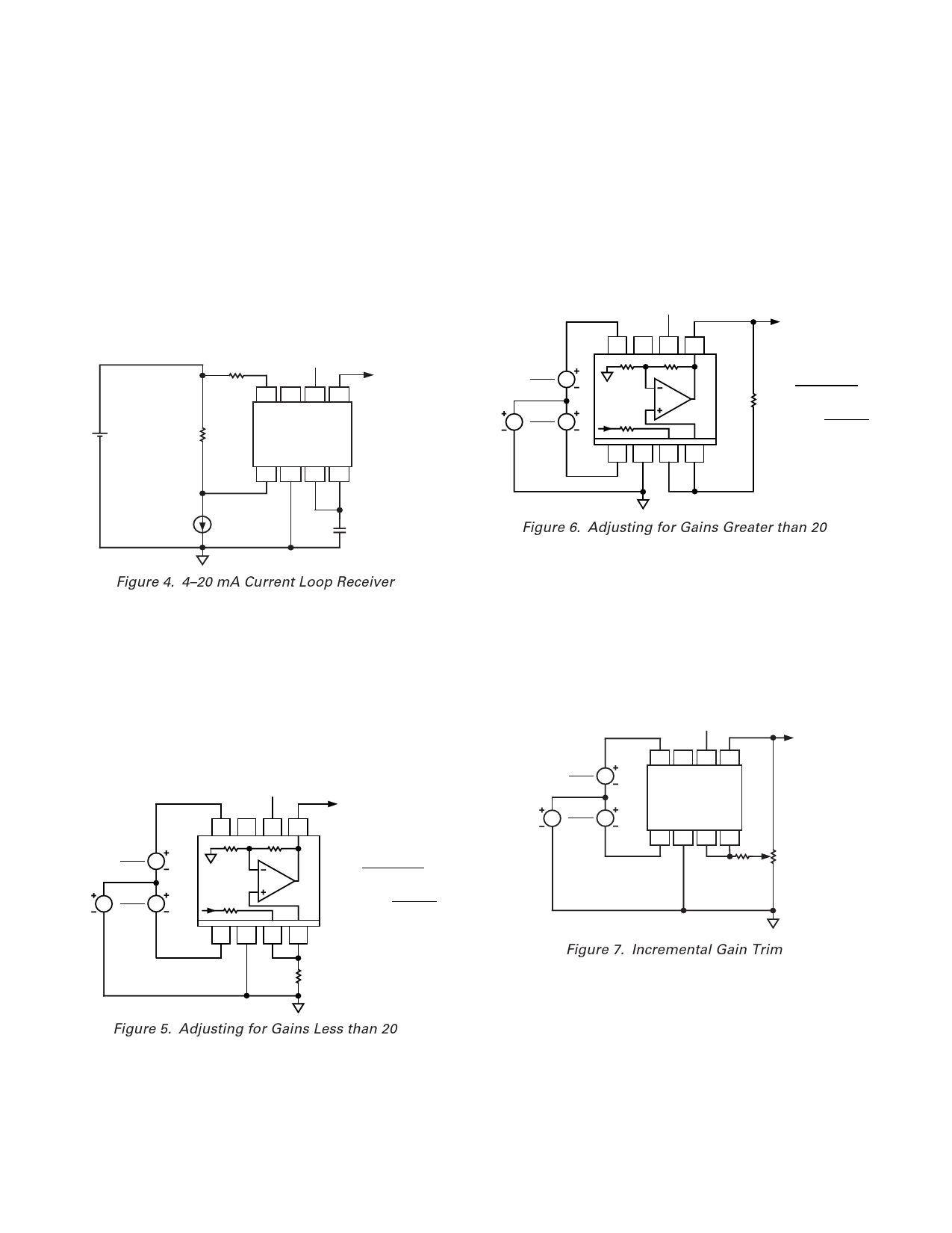
The AD8200 can also be used in low current sensing applica-
tions, such as the 4–20 mA current loop shown in Figure 4. In
such applications, the relatively large shunt resistor can degrade
the common-mode rejection. Adding a resistor of equal value in
the low impedance side of the input corrects for this error.
10⍀
5V
1%
+IN NC +VS OUT
OUTPUT
+
10⍀
1%
AD8200
–IN GND A1 A2
Gains Greater than 20
Connecting a resistor from the output of the buffer amplifier to
its noninverting input, as shown in Figure 6, will increase the
gain. The gain is now multiplied by the factor REXT/(REXT –
100 kΩ); for example, it is doubled for REXT = 200 kΩ. Overall
gains as high as 50 are achievable in this way. Note that the
accuracy of the gain becomes critically dependent on resistor
value at high gains. Also, the effective input offset voltage at
Pins 1 and 8 (about six times the actual offset of A1) limits the
part’s use in very high gain, dc-coupled applications.
VCM
VDIFF
2
VDIFF
2
+VS
+IN NC +VS OUT
OUT
10k⍀ 10k⍀
AD8200
100k⍀
REXT
GAIN = 20REXT
REXT – 100k⍀
REXT
=
100k⍀
GAIN
GAIN – 20
–IN GND A1 A2
NC = NO CONNECT
Figure 6. Adjusting for Gains Greater than 20
NC = NO CONNECT
Figure 4. 4–20 mA Current Loop Receiver
GAIN ADJUSTMENT
The default gain of the preamplifier and buffer are ϫ10 and ϫ2,
respectively, resulting in a composite gain of ϫ20. With the
addition of external resistor(s) or trimmer(s), the gain may be
lowered, raised, or finely calibrated.
Gains Less than 20
Since the preamplifier has an output resistance of 100 kΩ, an exter-
nal resistor connected from Pins 3 and 4 to GND will decrease the
gain by a factor REXT/(100 kΩ + REXT) (see Figure 5).
VCM
VDIFF
2
VDIFF
2
+VS
+IN NC +VS OUT
OUT
10k⍀ 10k⍀
AD8200
100k⍀
GAIN
=
20REXT
REXT + 100k⍀
REXT
=
100k⍀
GAIN
20 – GAIN
–IN GND A1 A2
REXT
GAIN TRIM
Figure 7 shows a method for incremental gain trimming using a
trimpot and external resistor REXT.
The following approximation is useful for small gain ranges
( ) ∆G ≈ 10MΩ ÷ REXT %
Thus, the adjustment range would be ± 2% for REXT = 5 MΩ;
± 10% for REXT = 1 MΩ, and so on.
VCM
VDIFF
2
VDIFF
2
5V
+IN NC +VS OUT
AD8200
OUT
–IN GND A1 A2
REXT
GAIN TRIM
20k⍀ MIN
NC = NO CONNECT
Figure 7. Incremental Gain Trim
NC = NO CONNECT
Figure 5. Adjusting for Gains Less than 20
The overall bandwidth is unaffected by changes in gain using
this method, although there may be a small offset voltage due to
the imbalance in source resistances at the input to the buffer. In
many cases this can be ignored, but if desired, can be nulled by
inserting a resistor equal to 100 kΩ minus the parallel sum of
REXT and 100 kΩ, in series with Pin 4. For example, with REXT
= 100 kΩ (yielding a composite gain of ϫ10), the optional offset
nulling resistor is 50 kΩ (see Figure 11.)
–6–
REV. B
Share Link: 