AD7920BRM データシートの表示(PDF) - Analog Devices
部品番号
コンポーネント説明
メーカー
AD7920BRM Datasheet PDF : 24 Pages
| |||
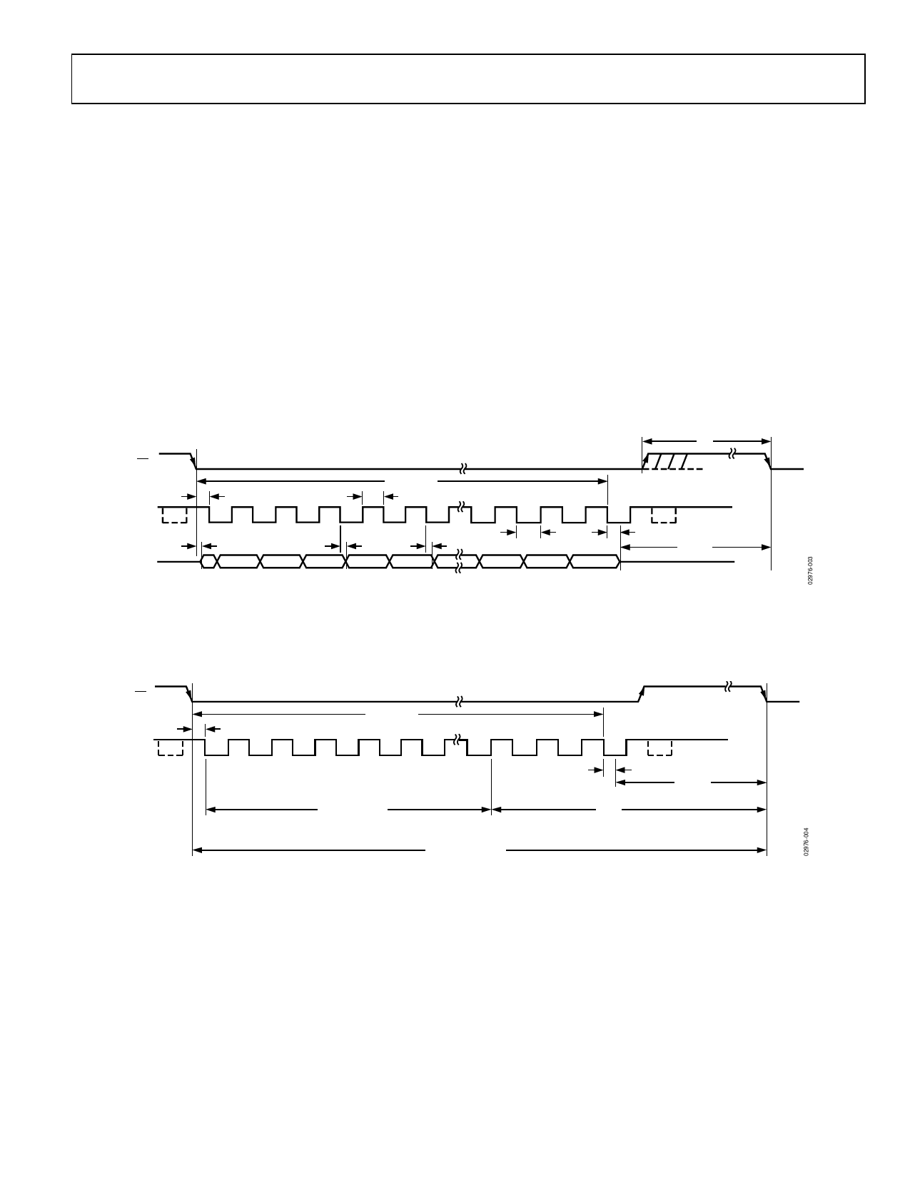
TIMING EXAMPLES
Figure 3 and Figure 4 show some of the timing parameters from
Table 3.
TIMING EXAMPLE 1
From Figure 4, having fSCLK = 5 MHz and a throughput rate of
250 kSPS gives a cycle time of t2 + 12.5(1/fSCLK) + tACQ = 4 μs.
With t2 = 10 ns min, this leaves tACQ to be 1.49 μs. This 1.49 μs
satisfies the requirement of 250 ns for tACQ. From Figure 4, tACQ
comprises 2.5(1/fSCLK) + t8 + tQUIET, where t8 = 36 ns max. This
allows a value of 954 ns for tQUIET, satisfying the minimum
requirement of 50 ns.
AD7910/AD7920
TIMING EXAMPLE 2
The AD7920 can also operate with slower clock frequencies.
From Figure 4, having fSCLK = 3.4 MHz and a throughput rate of
150 kSPS gives a cycle time of t2 + 12.5(1/fSCLK) + tACQ = 6.66 μs.
With t2 = 10 ns min, this leaves tACQ to be 2.97 μs. This 2.97 μs
satisfies the requirement of 250 ns for tACQ. From Figure 4, tACQ
comprises 2.5(1/fSCLK) + t8 + tQUIET, t8 = 36 ns max. This allows a
value of 2.19 μs for tQUIET, satisfying the minimum requirement
of 50 ns. As in this example and with other slower clock values,
the signal may already be acquired before the conversion is
complete, but it is still necessary to leave 50 ns minimum tQUIET
between conversions. In this example, the signal should be fully
acquired at approximately Point C in Figure 4.
CS
SCLK
tCONVERT
t2
t6
1
2
3
4
5
SDATA
THREE-
STATE
t3
Z ZERO
ZERO
t4
ZERO
4 LEADING ZEROS
DB11
t7
DB10
B
13
14
t5
15
16
t8
DB2
DB1
DB0
Figure 3. AD7920 Serial Interface Timing Diagram
t1
tQUIET
THREE-STATE
CS
SCLK
tCONVERT
t2
1
2
3
4
5
12.5(1/fSCLK)
B
C
13
14
15
16
t8
tACQ
1/THROUGHPUT
Figure 4. Serial Interface Timing Example
tQUIET
Rev. C | Page 7 of 24
Share Link: 