AD5122 データシートの表示(PDF) - Analog Devices
部品番号
コンポーネント説明
メーカー
AD5122 Datasheet PDF : 32 Pages
| |||
AD5122/AD5142
PIN CONFIGURATIONS AND FUNCTION DESCRIPTIONS
PIN 1
INDICATOR
GND 1
A1 2
W1 3
B1 4
AD5122/
AD5142
TOP VIEW
(Not to Scale)
12 SDI
11 SCLK
10 VLOGIC
9 VDD
Data Sheet
NOTES
1. EXPOSED PAD. CONNECT THE EXPOSED PAD TO THE
POTENTIAL OF THE VSS PIN, OR, ALTERNATIVELY, LEAVE
IT ELECTRICALLY UNCONNECTED. IT IS RECOMMENDED
THAT THE PAD BE THERMALLY CONNECTED TO A COPPER
PLANE FOR ENHANCED THERMAL PERFORMANCE.
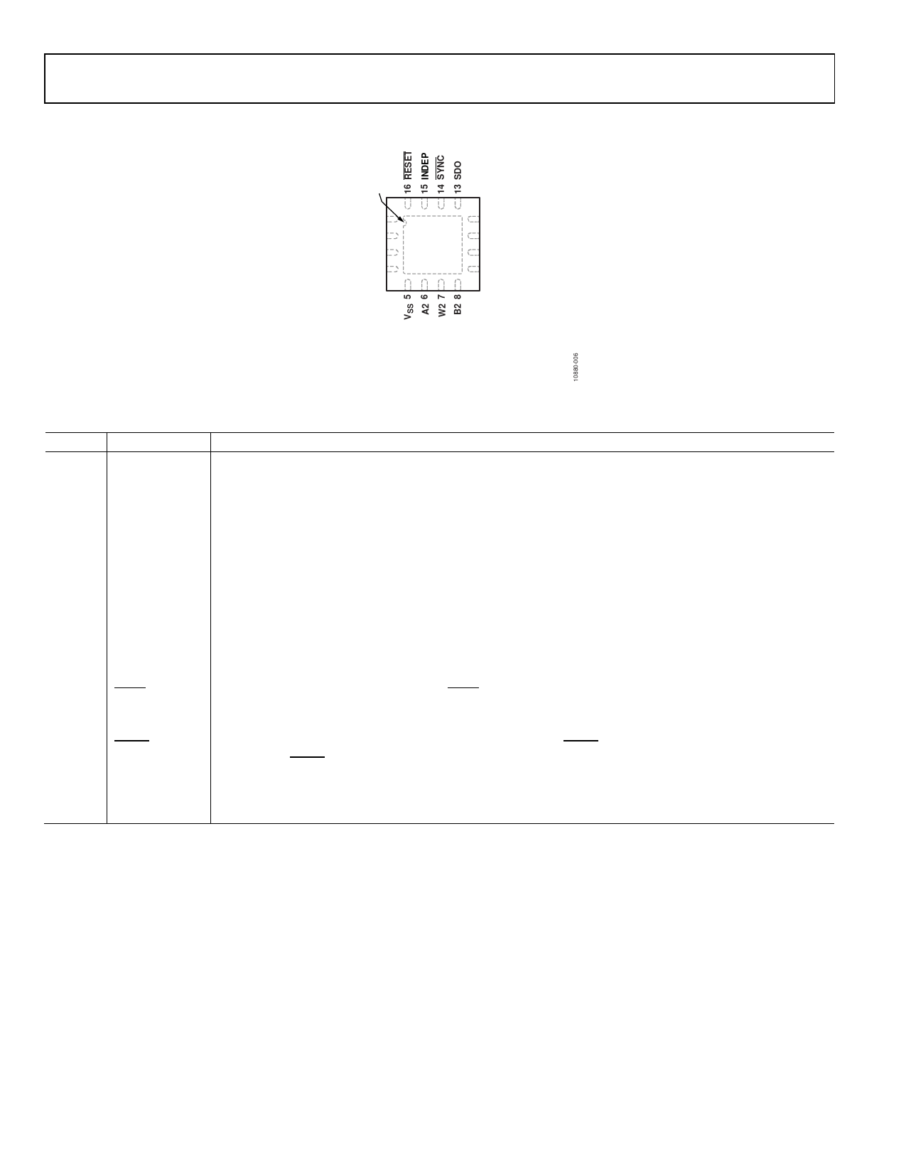
Figure 6. 16-Lead LFCSP Pin Configuration
Table 8. 16-Lead LFCSP Pin Function Descriptions
Pin No. Mnemonic
Description
1
GND
Ground Pin, Logic Ground Reference.
2
A1
3
W1
4
B1
5
VSS
6
A2
7
W2
8
B2
9
VDD
10
VLOGIC
11
SCLK
Terminal A of RDAC1. VSS ≤ VA ≤ VDD.
Wiper Terminal of RDAC1. VSS ≤ VW ≤ VDD.
Terminal B of RDAC1. VSS ≤ VB ≤ VDD.
Negative Power Supply. Decouple this pin with 0.1 µF ceramic capacitors and 10 µF capacitors.
Terminal A of RDAC2. VSS ≤ VA ≤ VDD.
Wiper Terminal of RDAC2. VSS ≤ VW ≤ VDD.
Terminal B of RDAC2. VSS ≤ VB ≤ VDD.
Positive Power Supply. Decouple this pin with 0.1 µF ceramic capacitors and 10 µF capacitors.
Logic Power Supply; 1.8 V to VDD. Decouple this pin with 0.1 µF ceramic capacitors and 10 µF capacitors.
Serial Clock Line. Data is clocked in at the logic low transition.
12
SDI
Serial Data Input.
13
SDO
Serial Data Output. This is an open-drain output pin, and it needs an external pull-up resistor.
14
SYNC
Synchronization Input, Active Low. When SYNC returns high, data is loaded into the input shift register.
15
INDEP
Linear Gain Setting Mode at Power-Up. Each string resistor is loaded independently from the associated
memory location. If INDEP is enabled, it cannot be disabled by software.
16
RESET
EPAD
Hardware Reset Pin. Refresh the RDAC registers from EEPROM. RESET is activated at the logic low. If this pin is
not used, tie RESET to VLOGIC.
Exposed Pad. Connect this exposed pad to the potential of the VSS pin, or, alternatively, leave it electrically
unconnected. It is recommended that the pad be thermally connected to a copper plane for enhanced
thermal performance.
Rev. C | Page 12 of 32
Share Link: 