A8507ELB データシートの表示(PDF) - Allegro MicroSystems
部品番号
コンポーネント説明
メーカー
A8507ELB Datasheet PDF : 16 Pages
| |||
A8507
LED Backlight Driver for LCD Monitors and Televisions
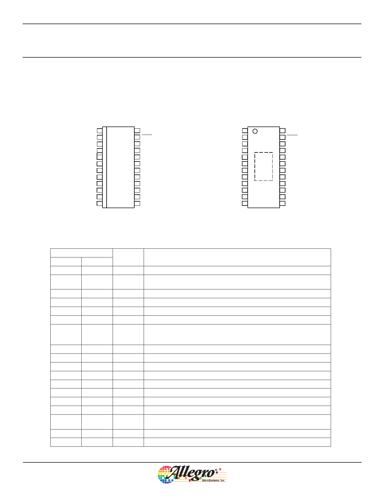
Pin-out Diagrams
PWM 1
PGND 2
NC 3
NC 4
SENN 5
GND 6
GND 7
SENP 8
OVP 9
DRIVER 10
VIN 11
ISET 12
24 EN
23 FAULT
22 LED6
21 LED5
20 LED4
19 LGND
18 LGND
17 LED3
16 LED2
15 LED1
14 COMP
13 FSET
Package LB
GND 1
PWM 2
NC 3
PGND 4
NC 5
SENN 6
SENP 7
OVP 8
NC 9
DRIVER 10
VIN 11
ISET 12
PAD
24 EN
23 FAULT
22 LED6
21 LED5
20 LED4
19 LGND
18 LED3
17 LED2
16 LED1
15 COMP
14 FSET
13 GND
Package LP
Terminal List Table
Number
LB
LP
1
2
2
4
3,4
3,5,9
5
6
6,7
1,13
8
7
9
8
10
11
12
13
14
15,16,17
18,19
20,21,22
23
24
–
10
11
12
14
15
16,17,18
19
20,21,22
23
24
PAD
Name
Function
PWM
PGND
NC
SENN
GND
SENP
OVP
DRIVER
VIN
ISET
FSET
COMP
LEDx
LGND
LEDx
¯F¯ ¯A ¯¯U ¯¯L¯ ¯T¯
EN
PAD
PWM LED-current control; apply logic level PWM for dimming
Power ground for external FET gate driver; connect to common star ground and
RSC ground
No internal electrical connection to these pins
Connect ground side of current sense resistor RSC
Connect to common star ground
Connect high side of current sense resistor RSC
Connect this pin to output capacitor +ve node to enable overvoltage protection;
typical OVP level is 36 V, and this level can be increased by connecting through
an external resistor ROVP
Gate driver terminal to drive external MOSFET
Input supply for the IC; decouple with a 0.1 μF ceramic capacitor
Sets 100% Current through LED strings; connect RISET from ISET to GND
Sets switching frequency; connect RFSET from FSET to GND
Compensation pin; connect 1 μF capacitor to GND or common star ground
LED sinks capable of 80 mA sink; connect unused LEDx pins to ground
Connect to common star ground
LED sinks capable of 80 mA sink; connect unused LEDx pins to ground
During normal operation, this pin is high (high impedance); at a fault event, this
pin pulls low
Device enable
Exposed pad for enhanced thermal dissipation, connect to common star ground
Allegro MicroSystems, Inc.
3
115 Northeast Cutoff
Worcester, Massachusetts 01615-0036 U.S.A.
1.508.853.5000; www.allegromicro.com
Share Link: 