74LVC1G10 データシートの表示(PDF) - Diodes Incorporated.
部品番号
コンポーネント説明
メーカー
74LVC1G10 Datasheet PDF : 13 Pages
| |||
74LVC1G10
SINGLE 3 INPUT POSITIVE NAND GATE
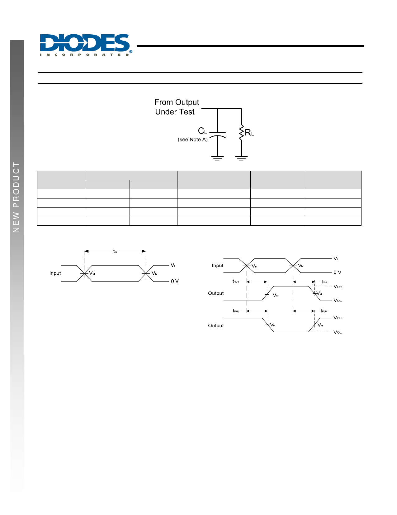
Parameter Measurement Information (cont.)
VCC
1.8V±0.15V
2.5V±0.2V
3.3V±0.3V
5V±0.5V
Inputs
VI
tr/tf
VCC
≤2ns
VCC
≤2ns
3V
≤2.5ns
VCC
≤2.5ns
VM
VCC/2
VCC/2
1.5V
VCC/2
CL
30pF
30pF
50pF
50pF
RL
1KΩ
500Ω
500Ω
500Ω
Voltage Waveform
Pulse Duration
Voltage Waveform
Propagation Delay Times
Inverting and Non Inverting Outputs
Figure 2. Load Circuit and Voltage Waveforms
Notes:
A . Includes test lead and test apparatus capacitance.
B. All pulses are supplied at pulse repetition rate ≤ 10 MHz
C. Inputs are measured separately one transition per measurement
D. tPLH and tPHL are the same as tPD
74LVC1G10
Document number: DS35121 Rev. 3 - 2
8 of 13
www.diodes.com
July 2011
© Diodes Incorporated
Share Link: 