74LVC1G10DW データシートの表示(PDF) - Diodes Incorporated.
部品番号
コンポーネント説明
メーカー
74LVC1G10DW Datasheet PDF : 14 Pages
| |||
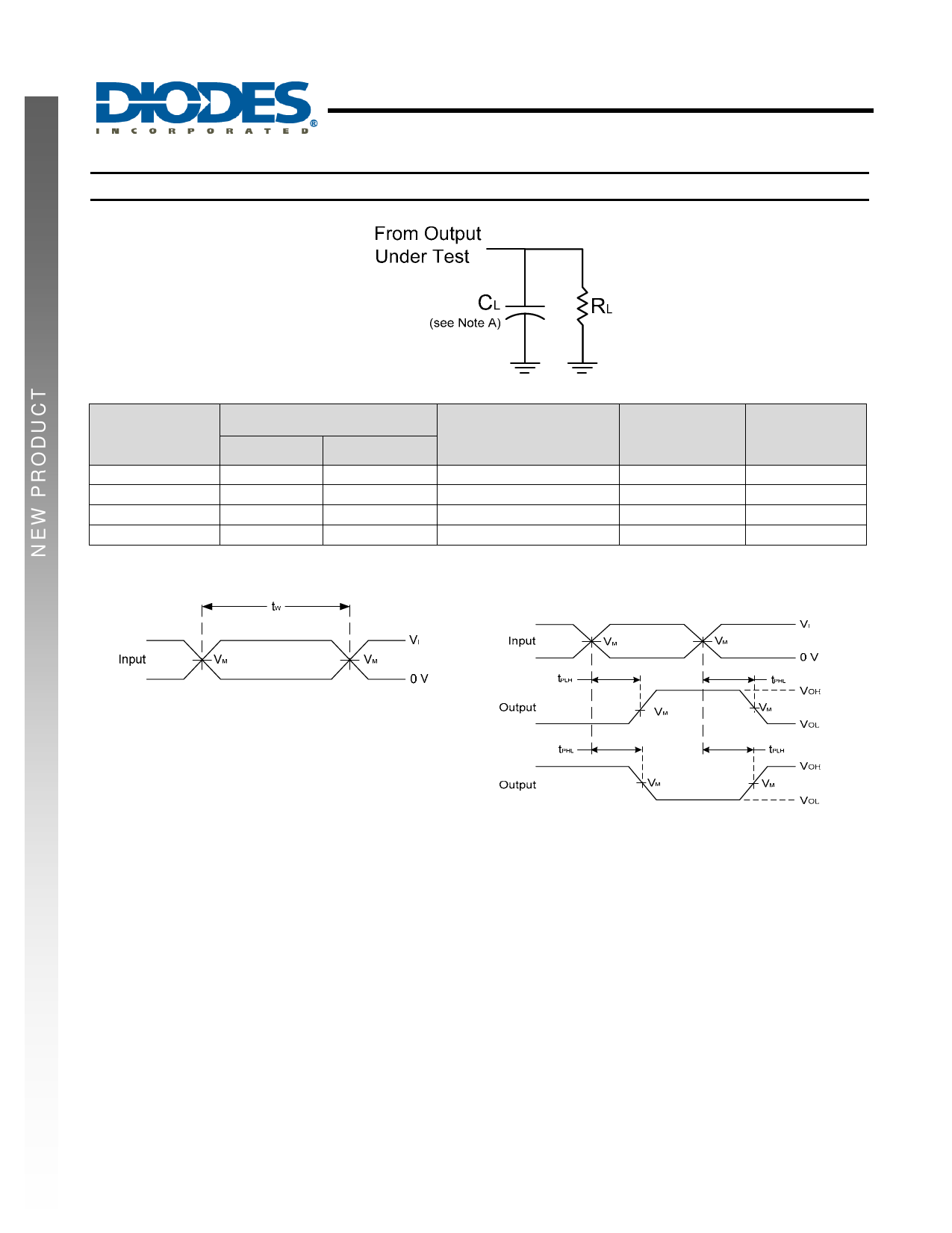
Parameter Measurement Information
74LVC1G10
SINGLE 3 INPUT POSITIVE NAND GATE
Vcc
1.8V±0.15V
2.5V±0.2V
3.3V±0.3V
5V±0.5V
Inputs
VI
tr/tf
VCC
≤2ns
VCC
≤2ns
3V
≤2.5ns
VCC
≤2.5ns
VM
VCC/2
VCC/2
1.5V
VCC/2
CL
15pF
15pF
15pF
15pF
RL
1MΩ
1MΩ
1MΩ
1MΩ
Voltage Waveform
Pulse Duration
Voltage Waveform
Propagation Delay Times
Inverting and Non Inverting Outputs
Notes:
A. Includes test lead and test apparatus capacitance.
B. All pulses are supplied at pulse repetition rate ≤ 10 MHz
C. Inputs are measured separately one transition per measurement
D. tPLH and tPHL are the same as tPD
Figure 1. Load Circuit and Voltage Waveforms
74LVC1G10
Document number: DS35121 Rev. 1 - 2
7 of 14
www.diodes.com
December 2010
© Diodes Incorporated
Share Link: 