ACH16540DGG データシートの表示(PDF) - Philips Electronics
部品番号
コンポーネント説明
メーカー
ACH16540DGG
Philips Electronics
ACH16540DGG Datasheet PDF : 12 Pages
| |||
Philips Semiconductors
16-bit buffer/line driver, inverting,
5V input tolerant (3-State)
Product specification
74ALVCH16540
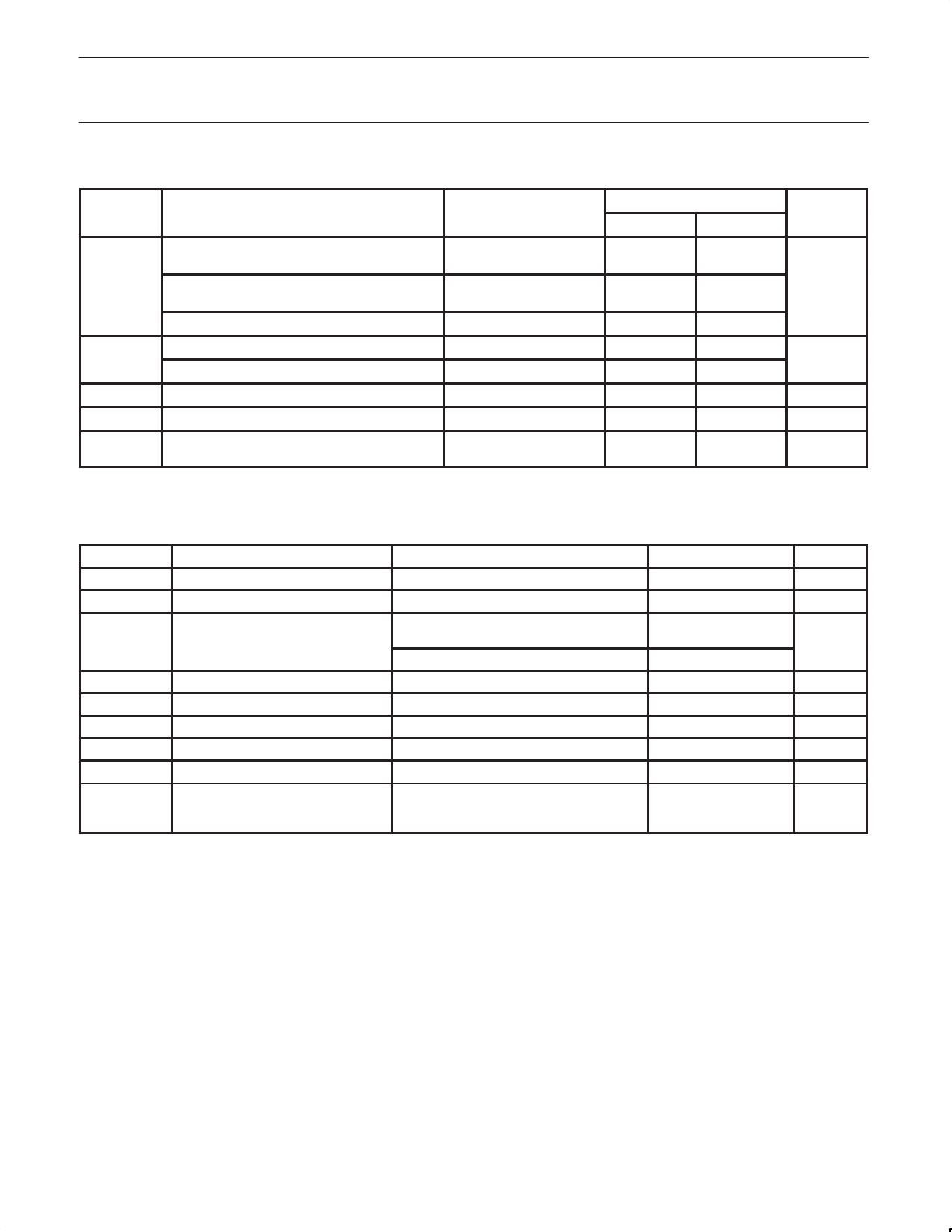
RECOMMENDED OPERATING CONDITIONS
SYMBOL
PARAMETER
VCC
VI
VO
Tamb
tr, tf
DC supply voltage 2.5V range (for max. speed
performance)
DC supply voltage 3.3V range (for max. speed
performance)
DC supply voltage (for low-voltage applications)
DC Input voltage range
DC Input voltage range
DC output voltage range
Operating free-air temperature range
Input rise and fall times
CONDITIONS
For data input pins
For control pins
VCC = 2.3 to 3.0V
VCC = 3.0 to 3.6V
LIMITS
MIN
MAX
2.3
2.7
3.0
3.6
1.2
3.6
0
VCC
0
5.5
0
VCC
–40
+85
0
20
0
10
UNIT
V
V
V
°C
ns/V
ABSOLUTE MAXIMUM RATINGS1, 2
In accordance with the Absolute Maximum Rating System (IEC 134)
Voltages are referenced to GND (ground = 0V)
SYMBOL
PARAMETER
CONDITIONS
RATING
UNIT
VCC
DC supply voltage
–0.5 to +4.6
V
IIK
DC input diode current
VI t0
–50
mA
VI
DC input voltage
For control pins and data inputs of ALVC
parts2
–0.5 to +5.5
V
For data inputs of ALVCH parts2
–0.5 to VCC +0.5
IOK
DC output diode current
VO uVCC or VO t 0
"50
mA
VO
DC output voltage
Note 2
–0.5 to VCC +0.5
V
IO
DC output source or sink current
VO = 0 to VCC
"50
mA
IGND, ICC DC VCC or GND current
"100
mA
Tstg
Storage temperature range
–65 to +150
°C
Power dissipation per package
For temperature range: –40 to +125 °C
PTOT
–plastic medium-shrink SO (SSOP) above +55°C derate linearly with 11.3 mW/K
850
mW
–plastic mini-pack (TSSOP)
above +55°C derate linearly with 8 mW/K
600
NOTES:
1. Stresses beyond those listed may cause permanent damage to the device. These are stress ratings only and functional operation of the
device at these or any other conditions beyond those indicated under “recommended operating conditions” is not implied. Exposure to
absolute-maximum-rated conditions for extended periods may affect device reliability.
2. The input and output voltage ratings may be exceeded if the input and output current ratings are observed.
1997 Aug 11
4
Share Link: 