74ABT833 データシートの表示(PDF) - Philips Electronics
部品番号
コンポーネント説明
メーカー
74ABT833 Datasheet PDF : 11 Pages
| |||
Philips Semiconductors
Octal transceiver with parity generator/checker
(3-State)
Product specification
74ABT833
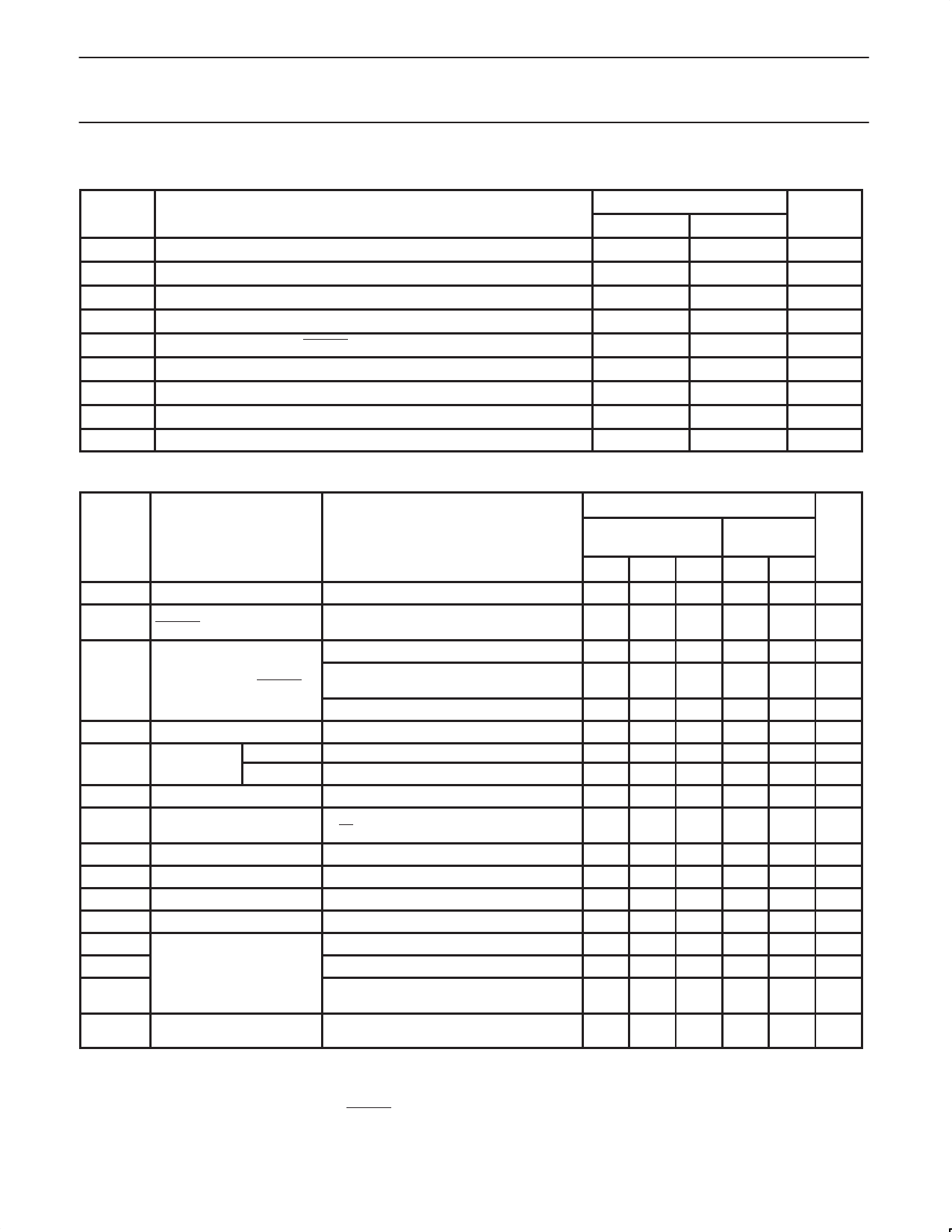
RECOMMENDED OPERATING CONDITIONS
SYMBOL
PARAMETER
VCC
VI
VIH
VIL
VOH
IOH
IOL
∆t/∆v
Tamb
DC supply voltage
Input voltage
High-level input voltage
Low-level input voltage
High-level output voltage, ERROR
High-level output current
Low-level output current
Input transition rise or fall rate
Operating free-air temperature range
LIMITS
Min
Max
4.5
5.5
0
VCC
2.0
0.8
5.5
–32
64
0
5
–40
+85
UNIT
V
V
V
V
V
mA
mA
ns/V
°C
DC ELECTRICAL CHARACTERISTICS
LIMITS
SYMBOL
PARAMETER
TEST CONDITIONS
Tamb = +25°C
Tamb = –40°C
to +85°C
UNIT
Min Typ Max Min Max
VIK
Input clamp voltage
IOH
High-level output current
ERROR ONLY
VCC = 4.5V; IIK = –18mA
VCC = 5.5V; VOH = 5.5V; VI = VIL or VIH
–0.9 –1.2
20
–1.2 V
20
µA
VCC = 4.5V; IOH = –3mA; VI = VIL or VIH
2.5 3.5
2.5
V
VOH
High-level output voltage
All outputs except ERROR
VCC = 5.0V; IOH = –3mA; VI = VIL or VIH
3.0 4.0
3.0
V
VCC = 4.5V; IOH = –32mA; VI = VIL or VIH
2.0 2.6
2.0
V
VOL
Low-level output voltage
VCC = 4.5V; IOL = 64mA; VI = VIL or VIH
0.42 0.55
0.55 V
II
Input leakage Control pins VCC = 5.5V; VI = GND or 5.5V
current
Data pins VCC = 5.5V; VI = GND or 5.5V
±0.01 ±1.0
±5 ±100
±1.0 µA
±100 µA
IOFF
Power-off leakage current
VCC = 0.0V; VI or VO ≤ 4.5V
±5.0 ±100
±100 V
IPUIPD
Power-up/down 3-State
output current3
VCC = 2.0V; or VO = 0.5V; VI = GND or VCC;
V OE = Don’t care
±5.0 ±50
±50
V
IIH + IOZH 3-State output High current VCC = 5.5V; VO = 2.7V; VI = VIL or VIH
5.0 50
50
µA
IIL + IOZL 3-State output Low current VCC = 5.5V; VO = 0.5V; VI = VIL or VIH
–5.0 –50
–50 µA
ICEX Output High leakage current VCC = 5.5V; VO = 5.5V; VI = GND or VCC
5.0 50
50
µA
IO
Output current1
VCC = 5.5V; VO = 2.5V
–50 –80 –180 –50 –180 mA
ICCH
VCC = 5.5V; Outputs High, VI = GND or VCC
50 250
250 µA
ICCL Quiescent supply current
VCC = 5.5V; Outputs Low, VI = GND or VCC
20
30
30 mA
ICCZ
VCC = 5.5V; Outputs 3-State;
VI = GND or VCC
50 250
250 µA
∆ICC
Additional supply current per VCC = 5.5V; one input at 3.4V,
input pin2
other inputs at VCC or GND
0.3 1.5
1.5 mA
NOTES:
1. Not more than one output should be tested at a time, and the duration of the test should not exceed one second.
2. This is the increase in supply current for each input at 3.4V.
3. This parameter is valid for any VCC between 0V and 2.1, with a transition time of up to 10msec. From VCC = 2.1V to VCC = 5V ± 10%, a
transition of up to 100µsec is permitted. The ERROR output pin 10 is not included in this spec due to the open collector design.
1993 Jun 21
5
Share Link: 