EVAL-AD7276CBZ データシートの表示(PDF) - Analog Devices
部品番号
コンポーネント説明
メーカー
EVAL-AD7276CBZ Datasheet PDF : 28 Pages
| |||
AD7276/AD7277/AD7278
AD7278 IN A 10 SCLK CYCLE SERIAL INTERFACE
For the AD7278, if CS is brought high during the 10th rising
edge after the two leading zeros and eight bits of the conversion
are provided, then the part can achieve a 4 MSPS throughput
rate. For the AD7278, the track-and-hold goes back into track
mode on the ninth rising edge. In this case, a fSCLK = 48 MHz and
throughput of 4 MSPS result in a cycle time of t2 + 8.5(1/fSCLK) +
tACQ = 250 ns, where t2 = 6 ns minimum and tACQ = 67 ns. This
satisfies the requirement of 60 ns for tACQ. Figure 35 shows that
tACQ comprises 0.5(1/fSCLK) + t8 + tQUIET, where t8 = 14 ns max.
This allows a value of 43 ns for tQUIET, satisfying the minimum
requirement of 4 ns.
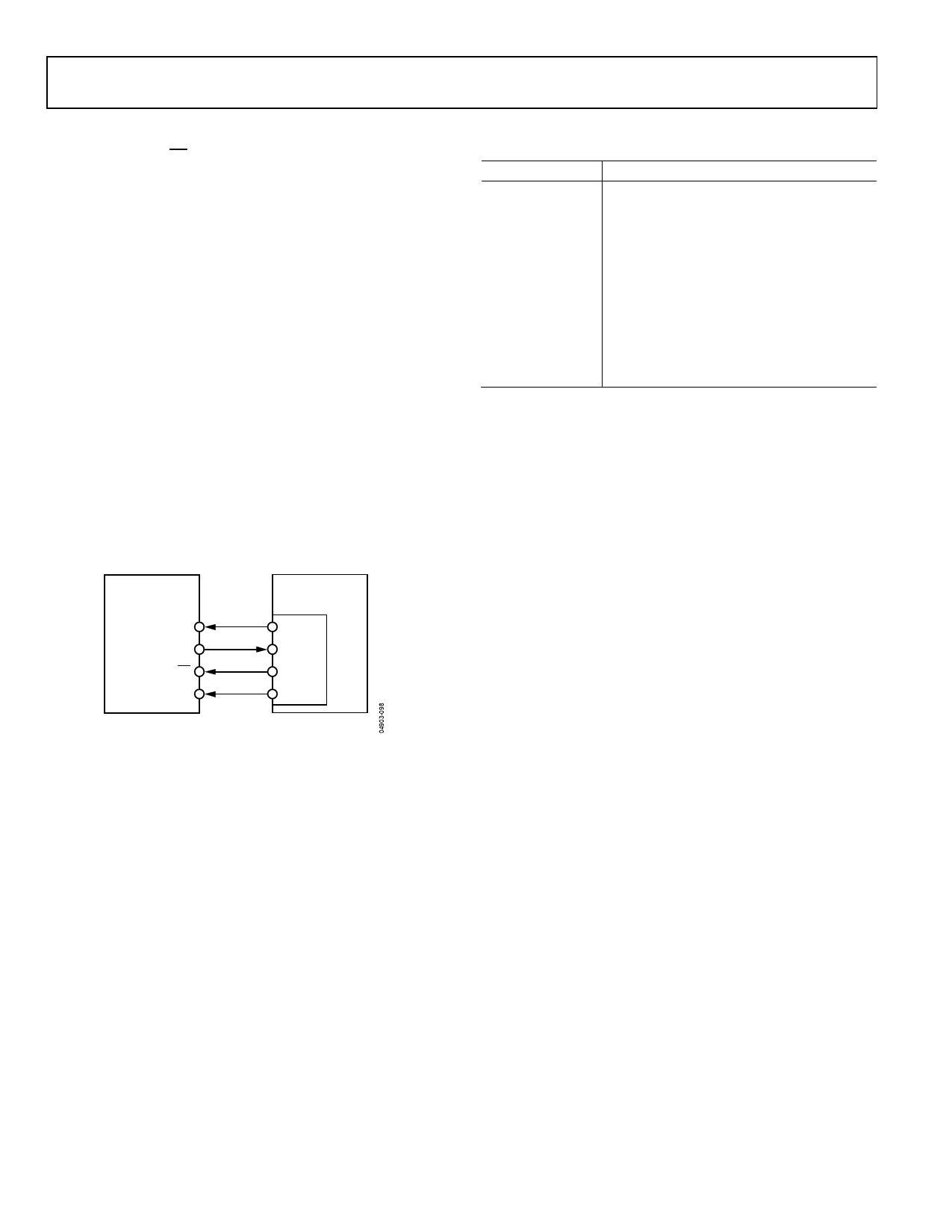
MICROPROCESSOR INTERFACING
AD7276/AD7277/AD7278 to Blackfin Processor
The Analog Devices, Inc., family of Blackfin DSPs, including
the ADSP-BF531, ADSP-BF532, ADSP-BF533, ADSP-BF534,
ADSP-BF535, ADSP-BF536, ADSP-BF537, ADSP-BF538,
ADSP-BF538F, ADSP-BF539, and ADSP-BF539F, interfaces
directly to the AD7276/AD7277/AD7278 without requiring
glue logic. (These DSPs are represented by the ADSP-BF531
in Figure 36.) Set up the SPORT0 Receive Configuration 1
Register up as outlined in Table 9.
AD7276/
AD7277/
AD7278*
SCLK
DOUT
CS
DIN
ADSP-BF531*
SPORT0
RSCLK0
DR0PRI
RFS0
DT0PRI
*ADDITIONAL PINS OMITTED FOR CLARITY
Figure 36. Interfacing with the ADSP-BF531
Data Sheet
Table 9. The SPORT0 Receive Configuration 1 Register
(SPORT0_RCR1)
Setting
Description
RCKFE = 1
Sample data with falling edge of RSCLK
LRFS = 1
Active low frame signal
RFSR = 1
Frame every word
IRFS = 1
Internal RFS used
RLSBIT = 0
Receive MSB first
RDTYPE = 00
Zero fill
IRCLK = 1
Internal receive clock
RSPEN = 1
Receive enabled
SLEN = 1111
16-bit data-word (or can be set to 1101 for
14-bit data-word)
TFSR = RFSR = 1
To implement the power-down modes, SLEN should be set to
1001 to issue an 8-bit SCLK burst.
Rev. E | Page 24 of 28
Share Link: 