LTC2298C Ver la hoja de datos (PDF) - Linear Technology
Número de pieza
componentes Descripción
fabricante
LTC2298C Datasheet PDF : 28 Pages
| |||
LTC2298/LTC2297/LTC2296
APPLICATIO S I FOR ATIO
Reference Operation
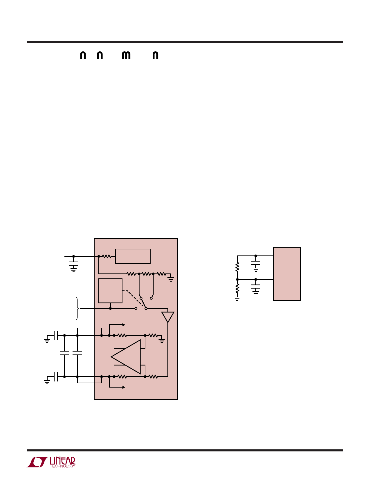
Figure 9 shows the LTC2298/LTC2297/LTC2296 refer-
ence circuitry consisting of a 1.5V bandgap reference, a
difference amplifier and switching and control circuit. The
internal voltage reference can be configured for two pin
selectable input ranges of 2V (±1V differential) or 1V
(±0.5V differential). Tying the SENSE pin to VDD selects
the 2V range; tying the SENSE pin to VCM selects the 1V
range.
The 1.5V bandgap reference serves two functions: its
output provides a DC bias point for setting the common
mode voltage of any external input circuitry; additionally,
the reference is used with a difference amplifier to gener-
ate the differential reference levels needed by the internal
ADC circuitry. An external bypass capacitor is required for
the 1.5V reference output, VCM. This provides a high
frequency low impedance path to ground for internal and
external circuitry.
LTC2298/LTC2297/LTC2296
1.5V
VCM
4Ω
1.5V BANDGAP
REFERENCE
2.2µF
1V 0.5V
TIE TO VDD FOR 2V RANGE;
TIE TO VCM FOR 1V RANGE;
RANGE = 2 • VSENSE FOR
0.5V < VSENSE < 1V
SENSE
1µF
REFH
RANGE
DETECT
AND
CONTROL
BUFFER
INTERNAL ADC
HIGH REFERENCE
2.2µF
1µF
0.1µF
REFL
DIFF AMP
INTERNAL ADC
LOW REFERENCE
229876 F09
Figure 9. Equivalent Reference Circuit
The difference amplifier generates the high and low refer-
ence for the ADC. High speed switching circuits are
connected to these outputs and they must be externally
bypassed. Each output has two pins. The multiple output
pins are needed to reduce package inductance. Bypass
capacitors must be connected as shown in Figure 9. Each
ADC channel has an independent reference with its own
bypass capacitors. The two channels can be used with the
same or different input ranges.
Other voltage ranges between the pin selectable ranges
can be programmed with two external resistors as shown
in Figure 10. An external reference can be used by applying
its output directly or through a resistor divider to SENSE.
It is not recommended to drive the SENSE pin with a logic
device. The SENSE pin should be tied to the appropriate
level as close to the converter as possible. If the SENSE pin
is driven externally, it should be bypassed to ground as
close to the device as possible with a 1µF ceramic capacitor.
For the best channel matching, connect an external reference
to SENSEA and SENSEB.
1.5V
12k
0.75V
12k
VCM
2.2µF
SENSE
1µF
LTC2298
LTC2297
LTC2296
229876 F10
Figure 10. 1.5V Range ADC
Input Range
The input range can be set based on the application. The
2V input range will provide the best signal-to-noise perfor-
mance while maintaining excellent SFDR. The 1V input
range will have better SFDR performance, but the SNR will
degrade by 5.8dB. See the Typical Performance Charac-
teristics section.
Driving the Clock Input
The CLK inputs can be driven directly with a CMOS or TTL
level signal. A sinusoidal clock can also be used along with
a low jitter squaring circuit before the CLK pin (Figure 11).
229876fa
19
Share Link: 