EL2360 Ver la hoja de datos (PDF) - Intersil
Número de pieza
componentes Descripción
fabricante
EL2360 Datasheet PDF : 14 Pages
| |||
EL2360
can be easily modified by varying the value of the feedback
resistor. For example, by reducing RF to 430Ω, bandwidth
can be extended to 170MHz with under 1dB of peaking.
Further reduction of RF to 360Ω increases the bandwidth to
195MHz with about 2.5dB of peaking.
Bandwidth vs Temperature
Whereas many amplifier’s supply current and consequently
-3dB bandwidth drop off at high temperature, the EL2360
was designed to have little supply current variation with
temperature. An immediate benefit from this is that the -3dB
bandwidth does not drop off drastically with temperature.
With VS = ±15V and AV = +2, the bandwidth varies only from
150MHz to 110MHz over the entire die junction temperature
range of -50°C < T < 150°C.
Supply Voltage Range and Single Supply
Operation
The EL2360 has been designed to operate with supply
voltages from ±2V to ±15V. Optimum bandwidth, slew rate,
and video characteristics are obtained at higher supply
voltages. However, at ±2V supplies, the -3dB bandwidth at
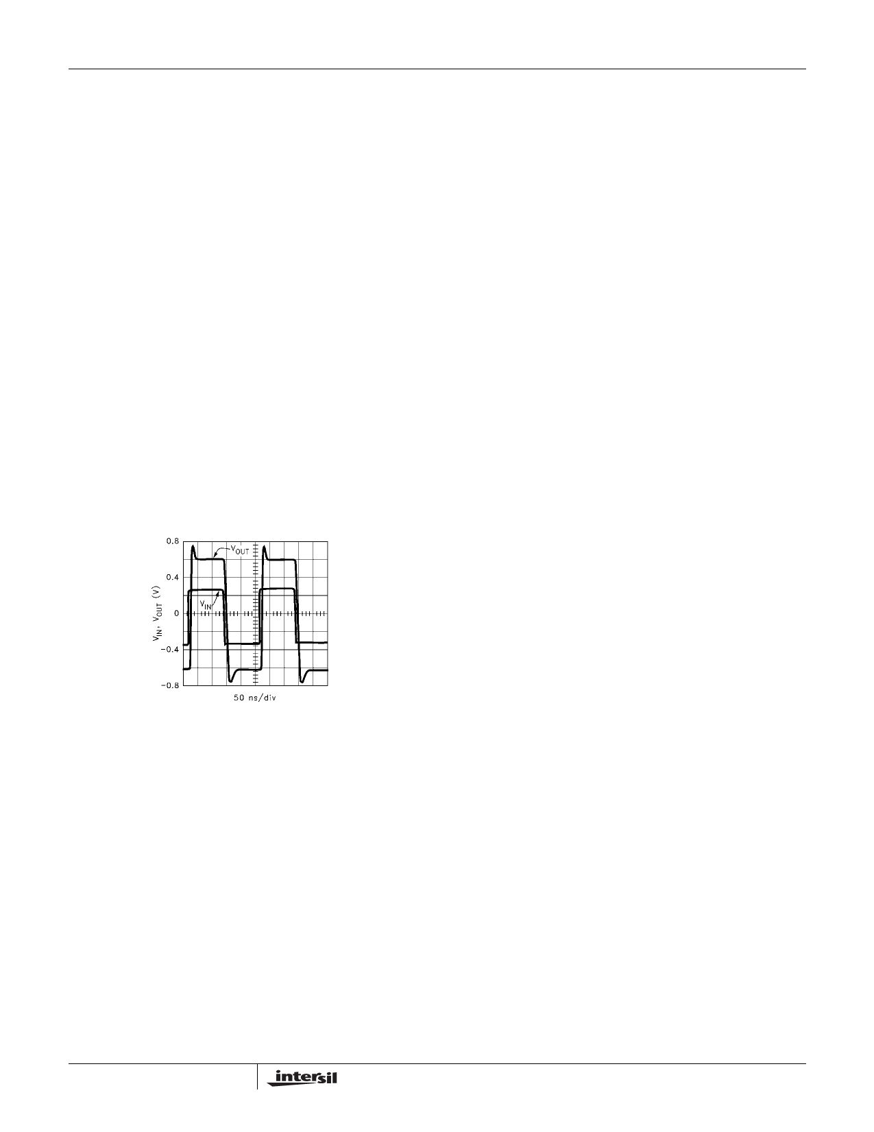
AV = +2 is a respectable 70MHz. The following figure is an
oscilloscope plot of the EL2360 at ±2V supplies, AV = +2,
RF = RG = 560Ω, driving a load of 150Ω, showing a clean
±600mV signal at the output.
caused by a power dissipation differential (before and after
the voltage step). For AV = -1, due to the inverting mode
configuration, this tail does not appear since the input stage
does not experience the large voltage change as in the non-
inverting mode. With AV = -1, 0.01% settling time is slightly
greater than 100ns.
Power Dissipation
The EL2360 amplifier combines both high speed and large
output current capability at a moderate supply current in very
small packages. It is possible to exceed the maximum
junction temperature allowed under certain supply voltage,
temperature, and loading conditions. To ensure that the
EL2360 remains within it’s absolute maximum ratings, the
following discussion will help to avoid exceeding the
maximum junction temperature.
The maximum power dissipation allowed in a package is
determined according to [1]:
PDMAX
=
T----J---M-----A----X-----–-----T----A---M-----A----X--
θJA
where:
TJMAX = Maximum Junction Temperature
TAMAX = Maximum Ambient Temperature
θJA = Thermal Resistance of the Package
PDMAX = Maximum Power Dissipation in the Package
The maximum power dissipation actually produced by an IC
is the total quiescent supply current times the total power
supply voltage, plus the power in the IC due to the load, or
[2] :
PDMAX
=
N
×
V S
×
ISMAX
+
(VS
–
VOUT)
×
-V----OR----UL----T--
If a single supply is desired, values from +4V to +30V can be
used as long as the input common mode range is not
exceeded. When using a single supply, be sure to either 1)
DC bias the inputs at an appropriate common mode voltage
and AC couple the signal, or 2) ensure the driving signal is
within the common mode range of the EL2360, which is
typically 1.5V from each supply rail.
Settling Characteristics
The EL2360 offers superb settling characteristics to 0.1%,
typically in the 35ns to 40ns range. There are no aberrations
created from the input stage which often cause longer
settling times in other current feedback amplifiers. The
EL2360 is not slew rate limited, therefore any size step up to
±10V gives approximately the same settling time.
As can be seen from the Long Term Settling Error curve, for
AV = +1, there is approximately a 0.035% residual which tails
away to 0.01% in about 40µs. This is a thermal settling error
where:
N =Number of amplifiers
VS = Total Supply Voltage
ISMAX = Maximum Supply Current per amplifier
VOUT = Maximum Output Voltage of the Application
RL = Load Resistance tied to Ground
If we set the two PDMAX equations, [1] and [2], equal to each
other, and solve for VS, we can get a family of curves for
various loads and output voltages according to [3]:
VS
=
-R---------L----------×--------(------T--------J--N----M--------×-A-------X--θ------J--–----A------T--------A--------M---------A-------X---------)----+-----(--V-----O----U----T----)--2-
(IS × RL) + VOUT
The figures below show total supply voltage VS vs RL for
various output voltage swings for the PDIP and SOIC
packages. The curves assume WORST CASE conditions of
TA = +85°C and IS = 11.3mA per amplifier. The curves do
11
Share Link: 