S593TRW Ver la hoja de datos (PDF) - Vishay Semiconductors
Número de pieza
componentes Descripción
fabricante
S593TRW Datasheet PDF : 10 Pages
| |||
S593T/S593TR/S593TRW
Vishay Semiconductors
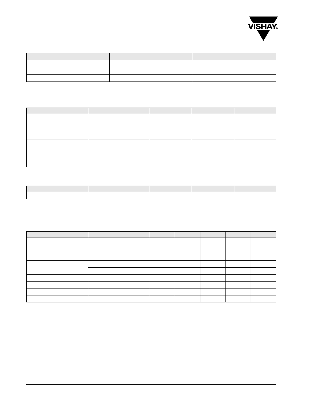
Parts Table
Part
S593T
S593TR
S593TRW
593
93R
W93
Marking
SOT-143
SOT-143R
SOT-343R
Package
Absolute Maximum Ratings
Tamb = 25 °C, unless otherwise specified
Parameter
Test condition
Drain - source voltage
Drain current
Gate 1/Gate 2 - source peak
current
Gate 1/Gate 2 - source voltage
Total power dissipation
Channel temperature
Tamb ≤ 60 °C
Storage temperature range
Symbol
Value
Unit
VDS
8
V
ID
30
mA
± IG1/G2SM
10
mA
± VG1/G2SM
6
V
Ptot
200
mW
TCh
150
°C
Tstg
- 55 to + 150
°C
Maximum Thermal Resistance
Parameter
Test condition
Symbol
Value
Unit
Channel ambient
1)
RthChA
450
K/W
1) on glass fibre printed board (25 x 20 x 1.5) mm3 plated with 35 μm Cu
Electrical DC Characteristics
Tamb = 25 °C, unless otherwise specified
Parameter
Test condition
Symbol
Min
Typ.
Max
Unit
Gate 1 - source breakdown
± IG1S = 10 mA, VG2S = VDS = 0 ± V(BR)G1SS
7
voltage
10
V
Gate 2 - source breakdown
± IG2S = 10 mA, VG1S = VDS = 0 ± V(BR)G2SS
7
voltage
10
V
Gate 1 - source leakage current + VG1S = 5 V, VG2S = VDS = 0
+ IG1SS
50
μA
- VG1S = 5 V, VG2S = VDS = 0
- IG1SS
100
μA
Gate 2 - source leakage current ± VG2S = 5 V, VG1S = VDS = 0
± IG2SS
20
nA
Drain current
VDS = 5 V, VG1S = 0, VG2S = 4 V
IDSS
50
500
μA
Self-biased operating current VDS = 5 V, VG1S = nc, VG2S = 4 V
IDSP
9
13
18
mA
Gate 2 - source cut-off voltage VDS = 5 V, VG1S = nc, ID = 20 μA VG2S(OFF)
1.0
V
Caution for Gate 1 switch-off mode:
No external DC-voltage on Gate 1 in active mode!
Switch-off at Gate 1 with VG1S < 0.7 V is feasible.
Using open collector switching transistor (inside of PLL), insert 10 kΩ collector resistor.
www.vishay.com
2
Document Number 85047
Rev. 1.6, 08-Sep-08
Share Link: 