MC10EP32_99 Ver la hoja de datos (PDF) - ON Semiconductor
Número de pieza
componentes Descripción
fabricante
MC10EP32_99 Datasheet PDF : 8 Pages
| |||
MC10EP32
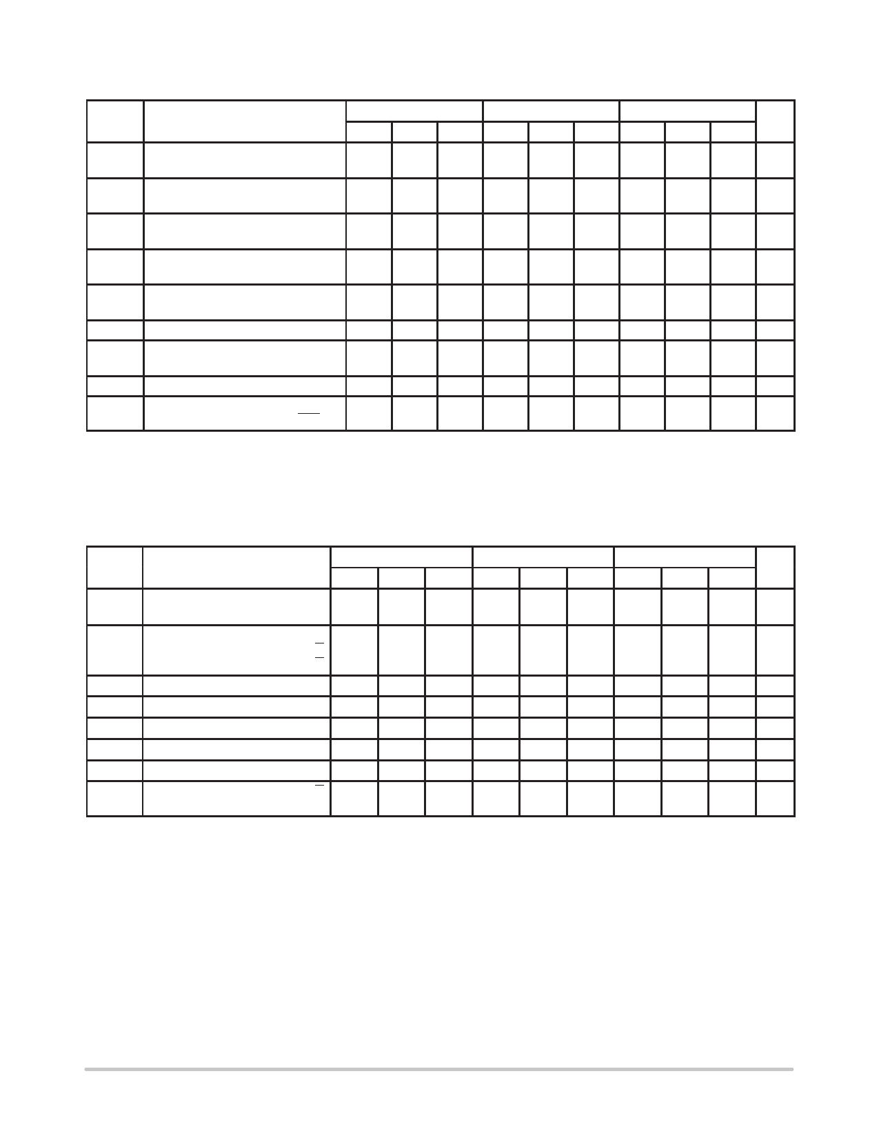
DC CHARACTERISTICS, PECL (VCC = 5.0V ± 0.5V, VEE = 0V) (Note 12.)
–40°C
25°C
85°C
Symbol
Characteristic
Min Typ Max Min Typ Max Min Typ Max Unit
IEE
Power Supply Current
(Note 9.)
23
30
37
23
30
37
23
30
37 mA
VOH
Output HIGH Voltage
(Note 10.)
3865 3940 4115 3930 4055 4180 3990 4115 4240 mV
VOL
Output LOW Voltage
(Note 10.)
3065 3190 3315 3130 3255 3380 3190 3315 3440 mV
VIH
Input HIGH Voltage
Single Ended
3790
4115 3855
4180 3915
4240 mV
VIL
Input LOW Voltage
Single Ended
3065
3390 3130
3455 3190
3515 mV
VBB
Output Voltage Reference
VIHCMR Input HIGH Voltage Common Mode
Range (Note 11.)
3490 3590 3690 3555 3655 3755 3615 3715 3815 mV
2.0
5.0
2.0
5.0
2.0
5.0
V
IIH
Input HIGH Current
IIL
Input LOW Current
CLK
0.5
CLK
–150
150
0.5
–150
150
0.5
–150
150 µA
µA
NOTE: 10EP circuits are designed to meet the DC specifications shown in the above table after thermal equilibrium has been established. The
circuit is in a test socket or mounted on a printed circuit board and transverse airflow greater than 500lfpm is maintained.
9. VCC = 5.0V, VEE = 0V, all other pins floating.
10. All loading with 50 ohms to VCC–2.0 volts.
11. VIHCMR min varies 1:1 with VEE, max varies 1:1 with VCC.
12. Input and output parameters vary 1:1 with VCC.
AC CHARACTERISTICS (VCC = 0V; VEE = –3.0V to –5.5V) or (VCC = 3.0V to 5.5V; VEE = 0V)
–40°C
25°C
85°C
Symbol
Characteristic
Min Typ Max Min Typ Max Min Typ Max Unit
fmax
Maximum Toggle Frequency
(Note 13.)
2.5
3.0
2.5
3.0
2.5
3.0
GHz
tPLH, Propagation Delay to
ps
tPHL
Output Differential CLK–>Q, Q 100
220
300 100
250
350
180
290
400
RESET–>Q, Q 100 220 300 100 250 350 180 290 400
tRR
Set/Reset Recovery
200 175
200 175
200 175
ps
tSKEW Duty Cycle Skew (Note 14.)
5.0
5.0
20
5.0
20
ps
tPW
Minimum Pulse Width RESET 550 475
550 475
550 475
ps
tJITTER Cycle–to–Cycle Jitter
TBD
TBD
TBD
ps
VPP
Input Voltage Swing (Diff.)
150 800 1200 150 800 1200 150 800 1200 mV
tr
Output Rise/Fall Times
Q, Q 50
100 150
70
120 170
70
130 200 ps
tf
(20% – 80%)
13. Fmax guaranteed for functionality only. VOL and VOH levels are guaranteed at DC only.
14. Skew is measured between outputs under identical transitions. Duty cycle skew is defined only for differential operation when the delays
are measured from the cross point of the inputs to the cross point of the outputs.
http://onsemi.com
4
Share Link: 