UPD720101F1-EA8 Ver la hoja de datos (PDF) - NEC => Renesas Technology
Número de pieza
componentes Descripción
fabricante
UPD720101F1-EA8 Datasheet PDF : 36 Pages
| |||
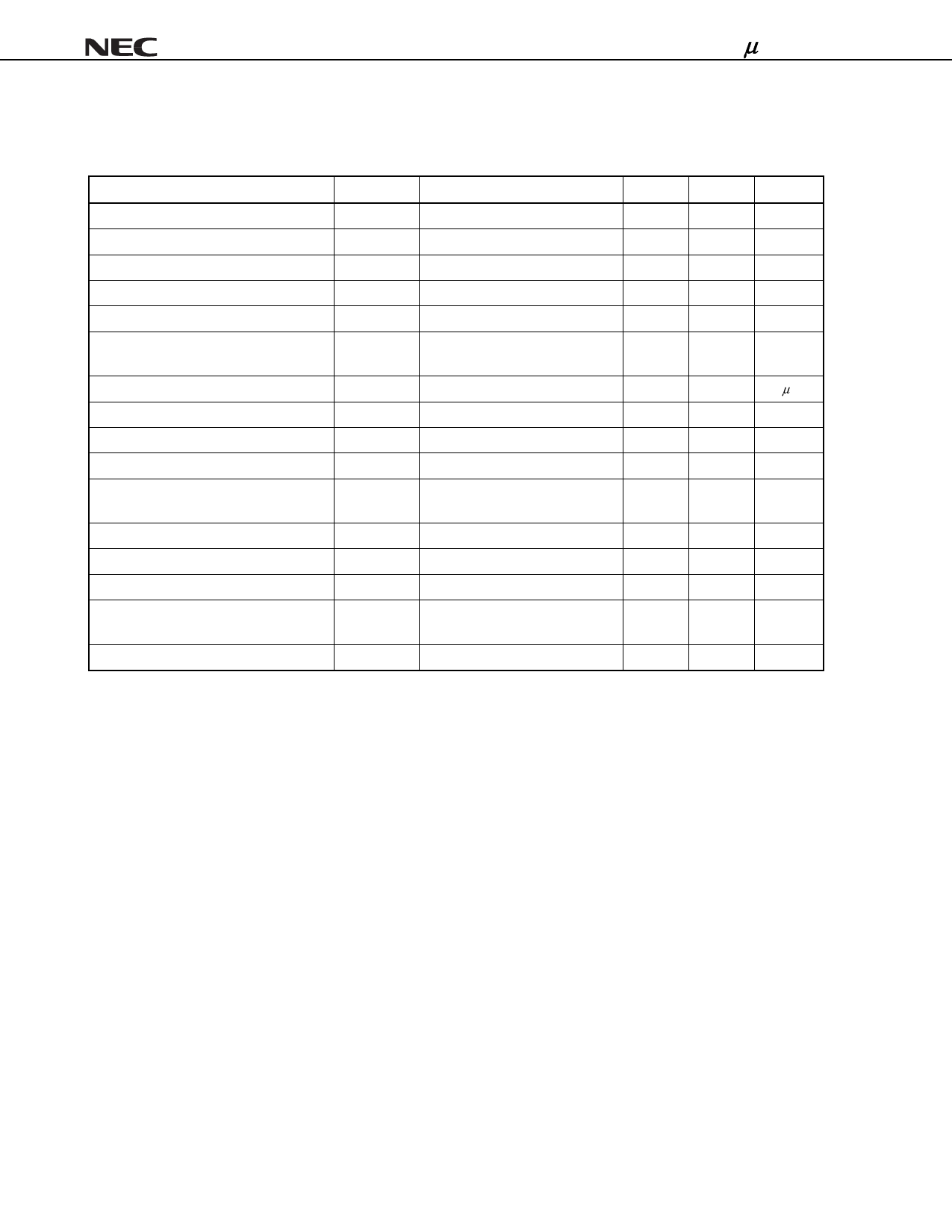
AC Characteristics (VDD = 3.0 to 3.6 V, TA = 0 to +70°C)
PCI interface block
Parameter
PCI clock cycle time
PCI clock pulse, high-level width
PCI clock pulse, low-level width
PCI clock, rise slew rate
PCI clock, fall slew rate
PCI reset active time (vs. power supply
stability)
PCI reset active time (vs. CLK start)
Output float delay time (vs. RST0↓)
PCI reset rise slew rate
PCI bus signal output time (vs. PCLK↑)
PCI point-to-point signal output time (vs.
PCLK↑)
Output delay time (vs. PCLK↑)
Output float delay time (vs. PCLK↑)
Input setup time (vs. PCLK↑)
Point-to-point input setup time (vs.
PCLK↑)
Input hold time
Symbol
tcyc
thigh
tlow
Scr
Scf
trst
trst-clk
trst-off
Srr
tval
tval (ptp)
ton
toff
tsu
tsu (ptp)
th
Condition
0.2VDD to 0.6VDD
0.2VDD to 0.6VDD
REQ0
GNT0
µPD720101
Min.
Max.
Unit
30
ns
11
ns
11
ns
1
4
V/ns
1
4
V/ns
1
ms
100
µs
40
ns
50
mV/ns
2
11
ns
2
12
ns
2
ns
28
ns
7
ns
10
ns
0
ns
22
Data Sheet S16265EJ4V0DS
Share Link: 