MAX9062EUK Ver la hoja de datos (PDF) - Maxim Integrated
Número de pieza
componentes Descripción
fabricante
MAX9062EUK
Maxim Integrated
MAX9062EUK Datasheet PDF : 12 Pages
| |||
Ultra-Small, Low-Power Single
Comparators in 4-Bump UCSP and 5 SOT23
Table 1. How Devices Behave Under Various Input Voltage Conditions
PART
MAX9060
MAX9061
MAX9062
MAX9063
MAX9064
INPUT VOLTAGE CONDITIONS
VIN > VREF
VIN < VREF
VIN > VREF
VIN < VREF
VIN > 0.2V
VIN < 0.2V
VIN > 0.2V
VIN < 0.2V
VIN > 0.2V
VIN < 0.2V
ACTION AT OUTPUT
External pullup resistor pulls output high.
Output asserts low.
Output asserts low.
External pullup resistor pulls output high.
External pullup resistor pulls output high.
Output asserts low.
Output asserts low.
External pullup resistor pulls output high.
Output asserts high.
Output asserts low.
Applications Information
Bypassing REF/VCC
Place a 0.1µF capacitor between REF or VCC and
GND as close as possible to the device. During a
switching event, all comparators draw a current spike
from their power-supply rails. This current spike is
minimized by the use of an internal break-before-make
design.
Hysteresis Operation
The MAX9060–MAX9064 feature internal hysteresis for
noise immunity and glitch-free operation. If additional
hysteresis is needed, an external positive feedback net-
work can be easily implemented on the MAX9060,
MAX9062, and MAX9064 noninverting input devices.
Additional external hysteresis is not recommended for
the MAX9061 due to possible crossover current-related
noise problems. Additional external hysteresis is not
possible on the MAX9063 because the noninverting
input of the comparator is not externally accessible.
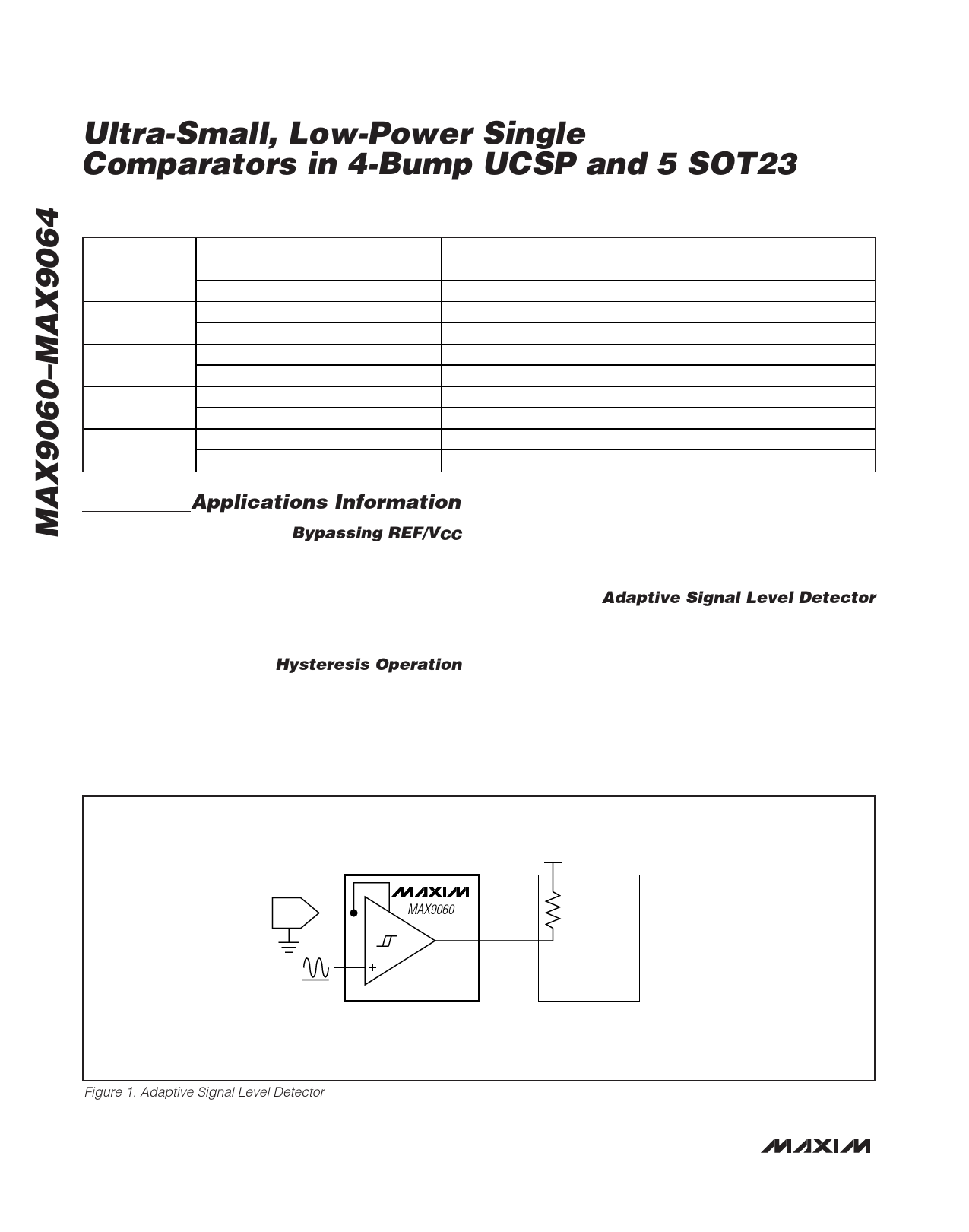
Adaptive Signal Level Detector
The MAX9060 and MAX9061 can be used as an adap-
tive signal-level detector. Feed a DAC output voltage
to REF and connect the input to a variable signal level.
As the DAC output voltage is varied from 0.9V to 5.5V,
a corresponding signal level threshold-detector circuit
is implemented. See Figure 1.
REF
DAC
IN
MAX9060
VDD
INTERNAL
PULLUP
OUT I/O
MICROCONTROLLER
Figure 1. Adaptive Signal Level Detector
8 _______________________________________________________________________________________
Share Link: 