SI4831 Ver la hoja de datos (PDF) - Silicon Laboratories
Número de pieza
componentes Descripción
fabricante
SI4831 Datasheet PDF : 20 Pages
| |||
Si4831/35-B30
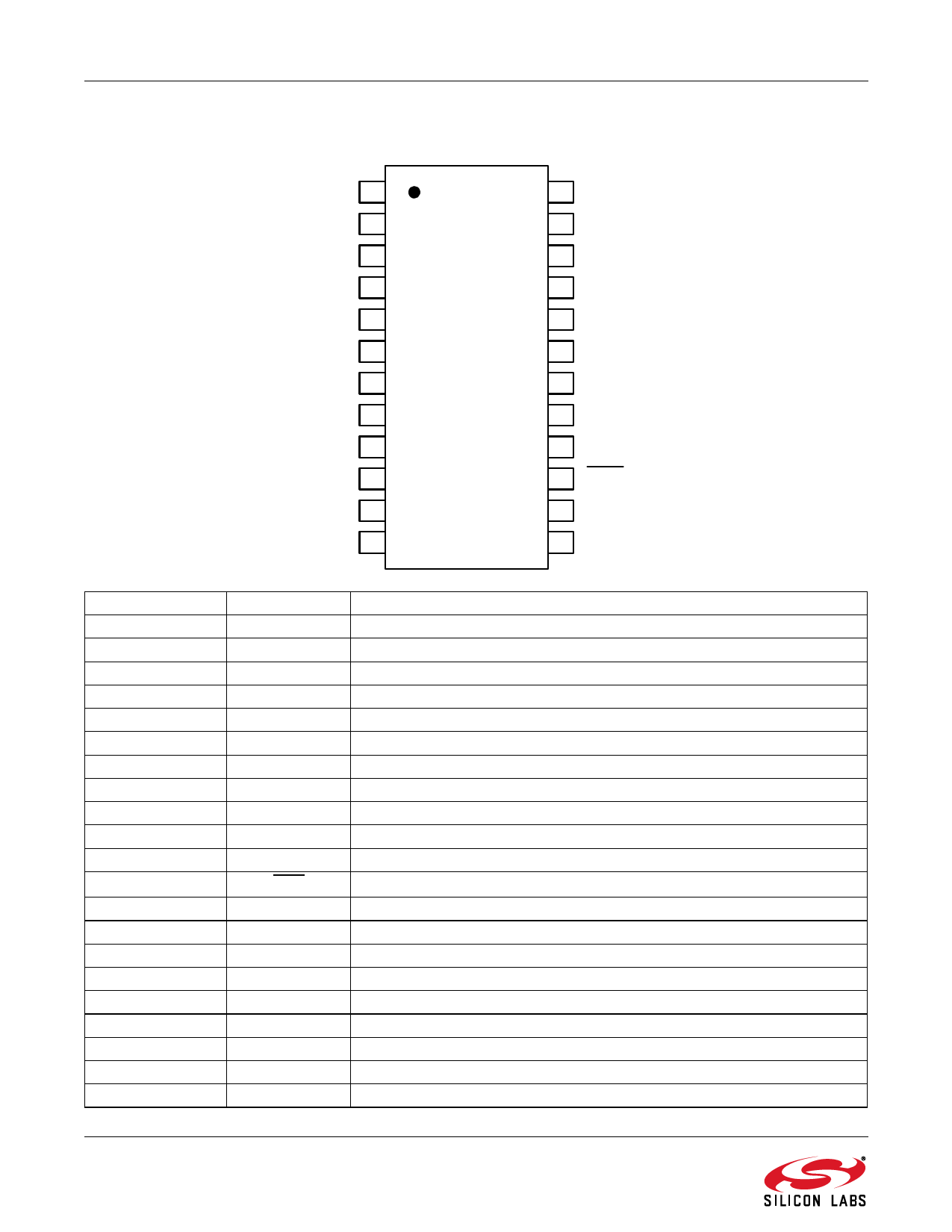
5. Pin Descriptions: Si4831/35-B30
STEREO
1
STATION
2
TUNE1
3
TUNE2
4
BAND
5
NC
6
NC
7
FMI
8
RFGND
9
NC
10
NC
11
AMI
12
24
LOUT
23
ROUT
22
DBYP
21
VDD2
20
VDD1
19
XTALI
18
XTALO
17
VOL-/BASS
16
VOL+/TREBLE
15
RST
14
GND
13
GND
Pin Number(s)
1
2
3
4
5
6,7
8
9
10,11
12
13,14
15
16
17
18
19
20
21
22
23
24
Name
Description
STEREO Stereo indicator
STATION Station indicator
TUNE1
Frequency tuning
TUNE2
Frequency tuning
BAND
Band selection and De-emphasis/Stereo separation selection
NC
No connect. Leave floating.
FMI
FM RF inputs. FMI should be connected to the antenna trace.
RFGND
RF ground. Connect to ground plane on PCB.
NC
Unused. Tie these pins to GND.
AMI
AM RF input. AMI should be connected to the AM antenna.
GND
Ground. Connect to ground plane on PCB.
RST
Device reset (active low) input
VOL+/TREBLE Volume button up/Treble
VOL–/BASS Volume button down/Bass
XTALO
Crystal oscillator output
XTALI
Crystal oscillator input
VDD1
Supply voltage. May be connected directly to battery.
VDD2
Supply voltage. May be connected directly to battery.
DBYP
Dedicated bypass for VDD
ROUT
Right audio line output in analog output mode
LOUT
Left audio line output in analog output mode
12
Rev. 1.0
Share Link: 