74HCT166(2015) Ver la hoja de datos (PDF) - NXP Semiconductors.
Número de pieza
componentes Descripción
fabricante
74HCT166 Datasheet PDF : 20 Pages
| |||
Nexperia
74HC166; 74HCT166
8-bit parallel-in/serial out shift register
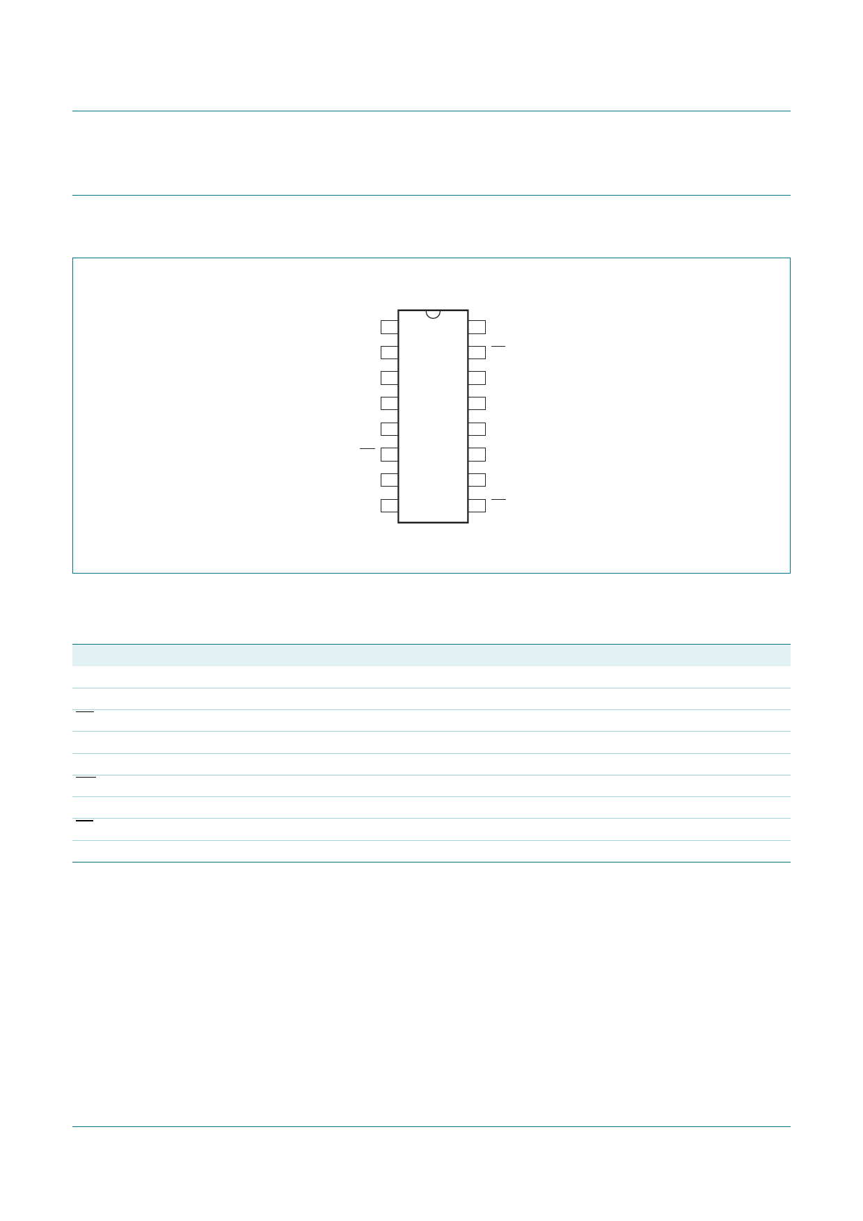
5. Pinning information
5.1 Pinning
+&
+&7
'6
'
'
'
'
&(
&3
*1'
Fig 5. Pin configuration SO16 and (T)SSOP16
9&&
3(
'
4
'
'
'
05
DDD
5.2 Pin description
Table 2.
Symbol
DS
D0 to D7
CE
CP
GND
MR
Q7
PE
VCC
Pin description
Pin
1
2, 3, 4, 5, 10, 11, 12, 14
6
7
8
9
13
15
16
Description
serial data input
parallel data inputs
clock enable input (active LOW)
clock input (LOW-to-HIGH edge-triggered)
ground (0 V)
asynchronous master reset (active LOW)
serial output from the last stage
parallel enable input (active LOW)
positive supply voltage
74HC_HCT166
Product data sheet
All information provided in this document is subject to legal disclaimers.
Rev. 4 — 28 December 2015
© Nexperia B.V. 2017. All rights reserved
4 of 20
Share Link: 