ID246 Ver la hoja de datos (PDF) - Sharp Electronics
Número de pieza
componentes Descripción
fabricante
ID246 Datasheet PDF : 38 Pages
| |||
SHARP
ID246 SERIES PRODUCT OVERVIEW
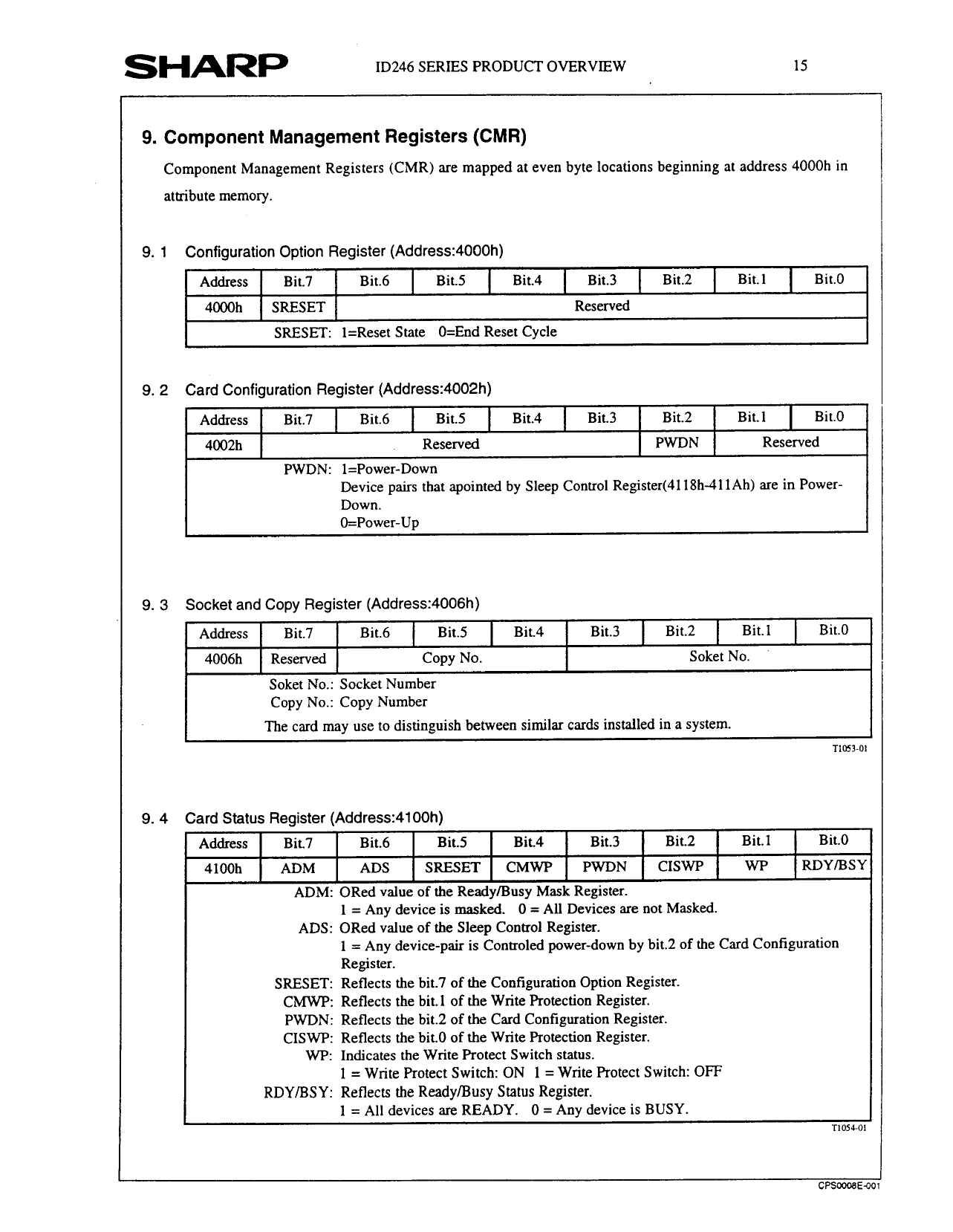
9. Component Management Registers (CMR)
Component Management Registers (CMR) are mapped at even byte locations beginning at address 4000h in
attribute memory.
9. 1 Configuration Option Register (Address:4000h)
Address
Bit.7
Bit.6
Bit.5
Bit.4
Bit.3
Bit.2
4000h SRESET
Reserved
SRESET: l=Reset State O=End Reset Cycle
Bit. 1
Bit.0
9. 2 Card Configuration Register (Address:4002h)
Address
4002h
Bit.7
PWDN:
Bit.6
Bit.5
Bit.4
Bit.3
Bit.2
Bit. 1
Bit.0
Reserved
PWDN
Reserved
l=Power-Down
Device pairs that apointed by Sleep Control Register(4118h-411 Ah) are in Power-
Down.
O=Power-Up
9. 3 Socket and Copy Register (Address:4006h)
Address
Bit.7
Bit.6
Bit.5
Bit.4
Bit.3
Bit.2
Bit.1
4006h Reserved
Copy No.
Soket No.
Soket No.: Socket Number
Copy No.: Copy Number
I
The card may use to distinguish between similar cards installed in a system.
Bit.0
TlOL-01
9. 4 Card Status Register (Address:41 OOh)
Address
Bit7
Bit.6
Bit.5
Bit.4
Bit.3
Bit.2
Bit.1
Bit.0
4100h
ADM
ADS
SRESET CMWP
PWDN
CISWP
WP RDYIBSY
ADM: ORed value of the Ready/Busy Mask Register.
1 = Any device is masked. 0 = All Devices are not Masked.
ADS: ORed value of the SleepControl Register.
1 = Any device-pair is Controledpower-down by bit.2 of the Card Configuration
Register.
SRESET: Reflects the bit.7 of the Configuration Option Register.
CMWP: Reflects the bit.1 of the Write Protection Register.
PWDN: Reflects the bit.2 of the Card Configuration Register.
CISWP: Reflects the bit.0 of the Write Protection Register.
WP: Indicates the Write Protect Switch status.
1 = Write Protect Switch: ON 1 = Write Protect Switch: OFF
RDY/BSY: Reflects the Ready/Busy StatusRegister.
1 = All devices are READY. 0 = Any device is BUSY.
TIO54-01
Share Link: 