CY8C4124LQQ-443 Ver la hoja de datos (PDF) - Cypress Semiconductor
Número de pieza
componentes Descripción
fabricante
CY8C4124LQQ-443 Datasheet PDF : 43 Pages
| |||
PSoC® 4: PSoC 4100 Family
Datasheet
Power
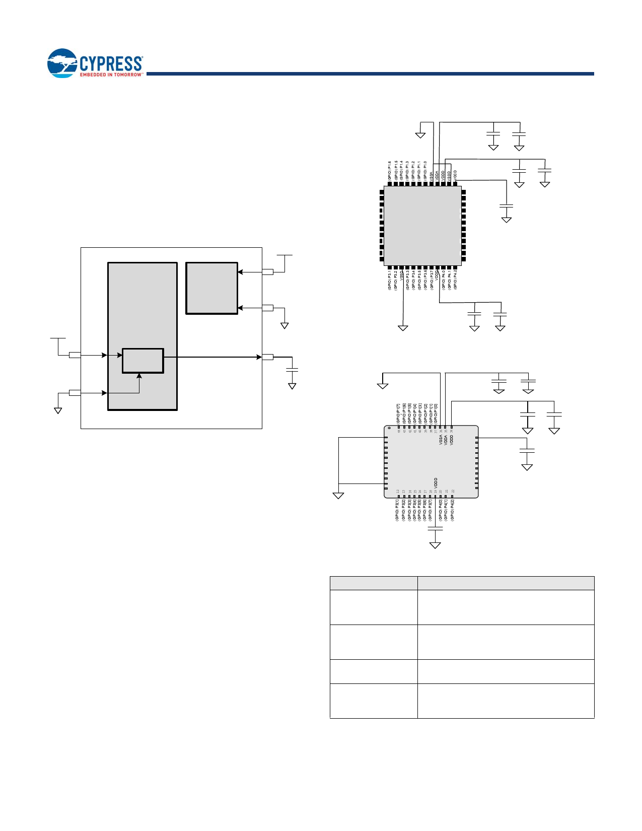
The following power system diagrams show the minimum set of
power supply pins as implemented for PSoC 4100. The system
has one regulator in Active mode for the digital circuitry. There is
no analog regulator; the analog circuits run directly from the
VDDA input. There are separate regulators for the Deep Sleep
and Hibernate (lowered power supply and retention) modes.
There is a separate low-noise regulator for the bandgap. The
supply voltage range is 1.71 V to 5.5 V with all functions and
circuits operating over that range.
Figure 10. PSoC 4 Power Supply
Digital
Domain
Analog
Domain
VDDA
VSSA
VDDA
VDDD
VDDD
VSSD
1.8 Volt
Reg
VCCD
The PSoC 4100 family allows two distinct modes of power supply
operation: Unregulated External Supply, and Regulated External
Supply modes.
Unregulated External Supply
In this mode, PSoC 4100 is powered by an external power supply
that can be anywhere in the range of 1.8 V to 5.5 V. This range
is also designed for battery-powered operation, for instance, the
chip can be powered from a battery system that starts at 3.5 V
and works down to 1.8 V. In this mode, the internal regulator of
PSoC 4100 supplies the internal logic and the VCCD output of the
PSoC 4100 must be bypassed to ground via an external
Capacitor (in the range of 1 µF to 1.6 µF; X5R ceramic or better).
VDDA and VDDD must be shorted together; the grounds, VSSA
and VSS must also be shorted together. Bypass capacitors must
be used from VDDD to ground, typical practice for systems in this
frequency range is to use a capacitor in the 1-µF range in parallel
with a smaller capacitor (0.1 µF for example). Note that these are
simply rules of thumb and that, for critical applications, the PCB
layout, lead inductance, and the Bypass capacitor parasitic
should be simulated to design and obtain optimal bypassing.
Figure 11. 48-TQFP Package Example
GROUND
0.1 µF C4
C3 1 µF
GROUND
1 µF C1
48 47 46 45 44 43 42 41 40 39 38 37
(GPIO)P1.7/VREF1 ?
36
(GPIO) P2.0 2
35
(GPIO) P2.1 3
34
(GPIO) P2.2 4
33
(GPIO) P2.3 5
(GPIO) P2.4 6
(GPIO) P2.5 7
48 TQFP
32
31
Top View
30
(GPIO) P2.6 8
29
(GPIO) P2.7 9
28
NC 10
27
NC 11
26
(GPIO) P3.0
12
25
13 14 15 16 17 18 19 20 21 22 23 24
XRES
(GPIO) P0.7
(GPIO) P0.6
(GPIO) P0.5
(GPIO) P0.4
(GPIO) P0.3
(GPIO) P0.2
(GPIO) P0.1
(GPIO) P0.0
NC
NC
(GPIO) P4.3
C5 1 µF
GROUND
C2 0.1 µF
GROUND
0.1 µF C4
GROUND
C3 1 µF
Figure 12. 44-TQFP Package Example
VSS
VSS
(G P IO )P 2 [0 ]
(G P IO )P 2 [1 ]
(G P IO )P 2[2 ]
(G P IO )P 2 [3 ]
(GPIO)P2[4]
(G P IO )P 2 [5 ]
(G P IO )P 2 [6 ]
(G P IO )P 2 [7 ]
(G P IO )P 3 [0 ]
1 VSS
2
3
4
5
6
7
8
9
10 VSS
11
0.1 µF C4
VSS
C3 1 µF
TQFP
(Top View)
1 µF C1
C2 0.1 µF
33 VCCD
32 XRES
31 (GPIO) P0[7]
30 (GPIO) P0[6]
29 (GPIO) P0[5]
28 (GPIO) P0[4]
27 (GPIO) P0[3]
26 (GPIO) P0[2]
25 (GPIO) P0[1]
24 (GPIO) P0[0]
23 (GPIO) P4[3]
VSS
C5 1 µF
VSS
C6 0.1 µF
VSS
Power Supply
VDDD–VSS
VDDA–VSSA
VCCD–VSS
VREF–VSSA
(optional)
Bypass Capacitors
0.1 µF ceramic at each pin (C2, C6) plus
bulk capacitor 1 to 10 µF (C1). Total capac-
itance may be greater than 10 µF.
0.1 µF ceramic at pin (C4). Additional
1 µF to 10 µF (C3) bulk capacitor. Total
capacitance may be greater than 10 µF.
1 µF ceramic capacitor at the VCCD pin
(C5)
The internal bandgap may be bypassed
with a 1 µF to 10 µF capacitor. Total capac-
itance may be greater than 10 µF.
Document Number: 001-87220 Rev. *J
Page 15 of 43
Share Link: 