WM8772EDS Ver la hoja de datos (PDF) - Wolfson Microelectronics plc
Número de pieza
componentes Descripción
fabricante
WM8772EDS Datasheet PDF : 70 Pages
| |||
Production Data
WM8772EDS – 28 PIN SSOP
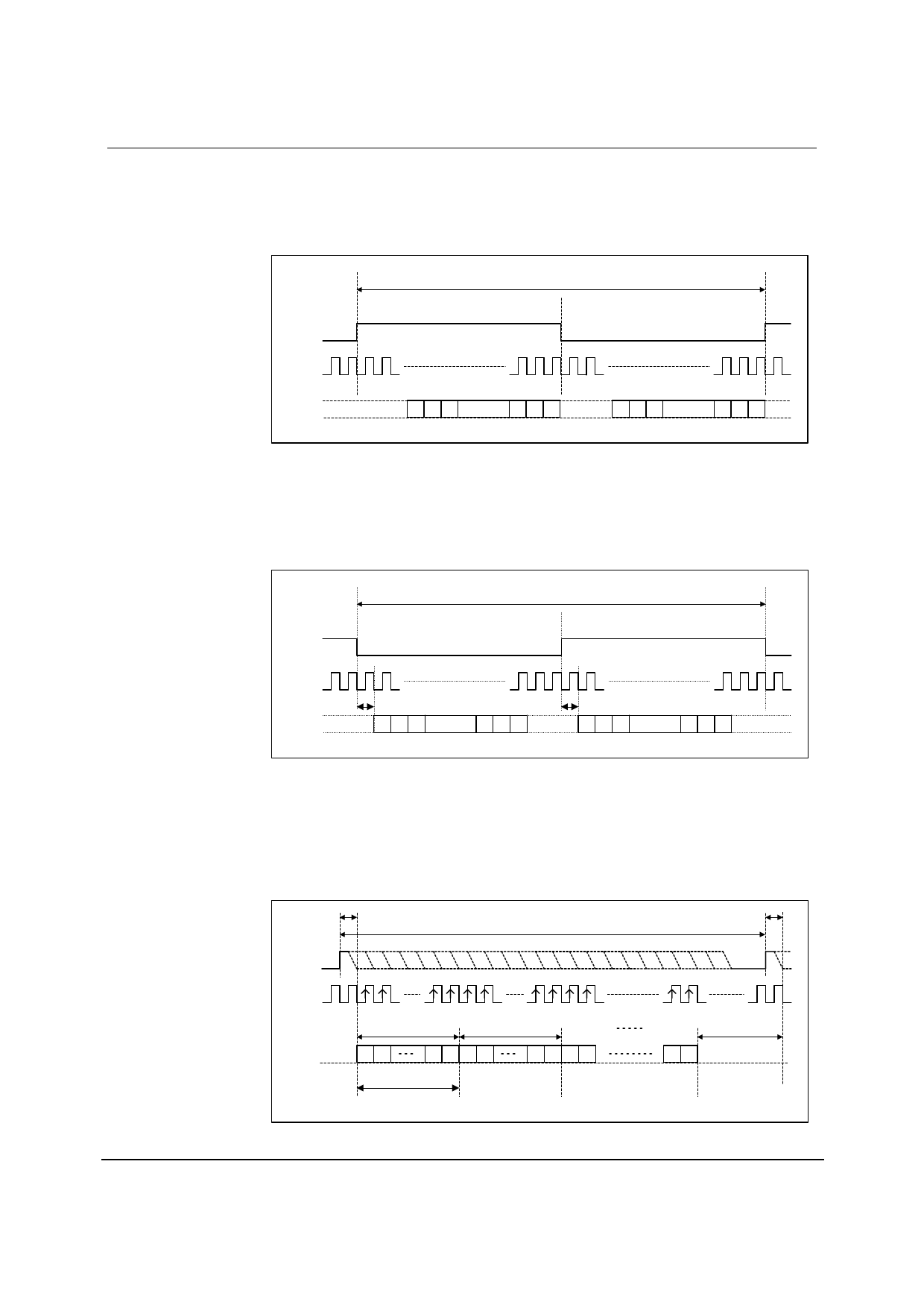
RIGHT JUSTIFIED MODE
In right justified mode, the LSB of DIN1/2/3 is sampled by the WM8772EDS on the rising edge of
BCLK preceding a LRC transition. The LSB of the ADC data is output on DOUT and changes on the
falling edge of BCLK preceding a LRC transition and may be sampled on the rising edge of BCLK.
LRC are high during the left samples and low during the right samples (Figure 24).
1/fs
DACLRC/
ADCLRC
DACBCLK/
ADCBCLK
LEFT CHANNEL
RIGHT CHANNEL
DIN1/2/3/
DOUT
123
MSB
n-2 n-1 n
LSB
123
MSB
n-2 n-1 n
LSB
Figure 24 Right Justified Mode Timing Diagram
I2S MODE
In I2S mode, the MSB of DIN1/2/3 is sampled by the WM8772EDS on the second rising edge of
BCLK following a LRC transition. The MSB of the ADC data is output on DOUT and changes on the
first falling edge of BCLK following an LRC transition and may be sampled on the rising edge of
BCLK. LRC are low during the left samples and high during the right samples.
1/fs
DACLRC/
ADCLRC
LEFT CHANNEL
DACBCLK/
ADCBCLK
DIN1/2/3/
DOUT
1 BCLK
123
MSB
n-2 n-1 n
LSB
Figure 25 I2S Mode Timing Diagram
RIGHT CHANNEL
1 BCLK
123
MSB
n-2 n-1 n
LSB
DSP EARLY MODE
In DSP early mode, the MSB of DAC channel 1 left data is sampled by the WM8772EDS on the
second rising edge on BCLK following a LRC rising edge. DAC channel 1 right and DAC channels 2
and 3 data follow DAC channel 1 left data (Figure 26).
DACLRC
DACBCLK
DIN1
1 BCLK
1/fs
1 BCLK
CHANNEL 1
LEFT
CHANNEL 1
RIGHT
CHANNEL 2
LEFT
12
MSB
n-1 n 1 2
LSB
n-1 n 1 2
Input Word Length (IWL)
CHANNEL 3
RIGHT
n-1 n
NO VALID DATA
Figure 26 DSP Early Mode Timing Diagram – DAC Data Input
w
PD Rev 4.1 October 2004
25
Share Link: 