QL7100-4PT208M Ver la hoja de datos (PDF) - QuickLogic Corporation
Número de pieza
componentes Descripción
fabricante
QL7100-4PT208M Datasheet PDF : 42 Pages
| |||
4/ (FOLSVH3OXV 'DWD 6KHHW
W W W W W W &RPELQLQJ 3HUIRUPDQFH 'HQVLW\ DQG (PEHGGHG 5$0
'HYLFH +LJKOLJKWV
)OH[LEOH 3URJUDPPDEOH /RJLF
.25 µm five layer metal CMOS Process
2.5 V VCC, 2.5/3.3 V Drive Capable I/O
960 Logic Cells
248,160 Max System Gates
Up to 250 I/O Pins
(PEHGGHG 'XDO 3RUW 65$0
Twenty 2,304-bit Dual Port High
Performance SRAM Blocks
46,100 RAM bits
RAM/ROM/FIFO Wizard for Automatic
Configuration
Configurable and Cascadable
3URJUDPPDEOH ,2
High performance Enhanced I/O (EIO)—
less than 3 ns Tco
Programmable Slew Rate Control
Programmable I/O Standards:
LVTTL, LVCMOS, PCI, GTL+, SSTL2,
and SSTL3
Eight Independent I/O Banks
Three Register Configurations: Input,
Output, and Output Enable
$GYDQFHG &ORFN 1HWZRUN
Nine Global Clock Networks:
One Dedicated
Eight Programmable
20 Quad-Net Networks—five per Quadrant
16 I/O Controls—two per I/O Bank
Four phase locked loops
(PEHGGHG &RPSXWDWLRQDO 8QLWV
ECUs provide integrated Multiply, Add, and
Accumulate Functions.
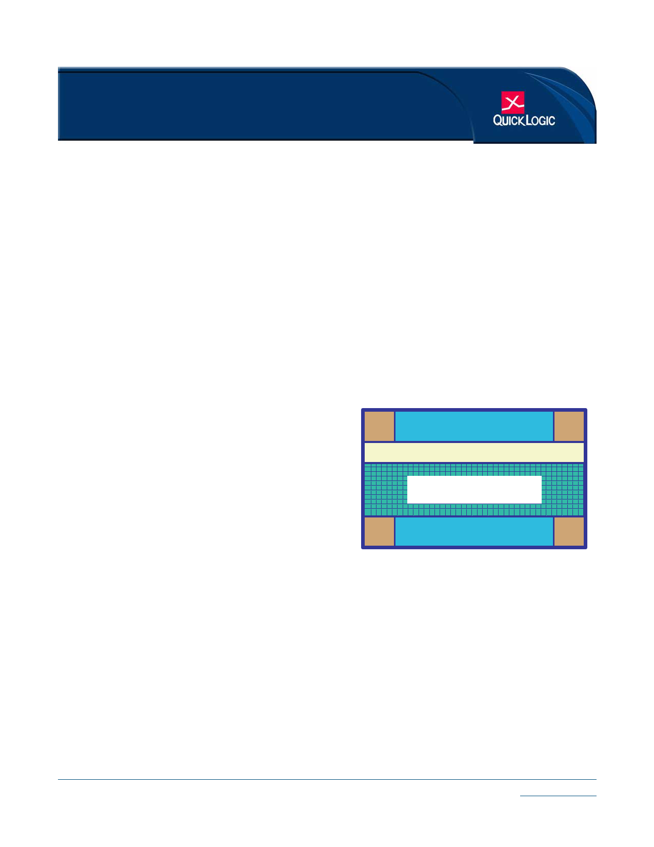
PLL
Memory - Dual Port RAM
PLL
Embedded Computational Units
High Speed Logic Cells
248K Gates
PLL
Memory - Dual Port RAM
PLL
)LJXUH
(FOLSVH3OXV %ORFN 'LDJUDP
4XLFN/RJLF &RUSRUDWLRQ
ZZZTXLFNORJLFFRP WWWWWW
Share Link: 