TDA7500A Ver la hoja de datos (PDF) - STMicroelectronics
Número de pieza
componentes Descripción
fabricante
TDA7500A Datasheet PDF : 41 Pages
| |||
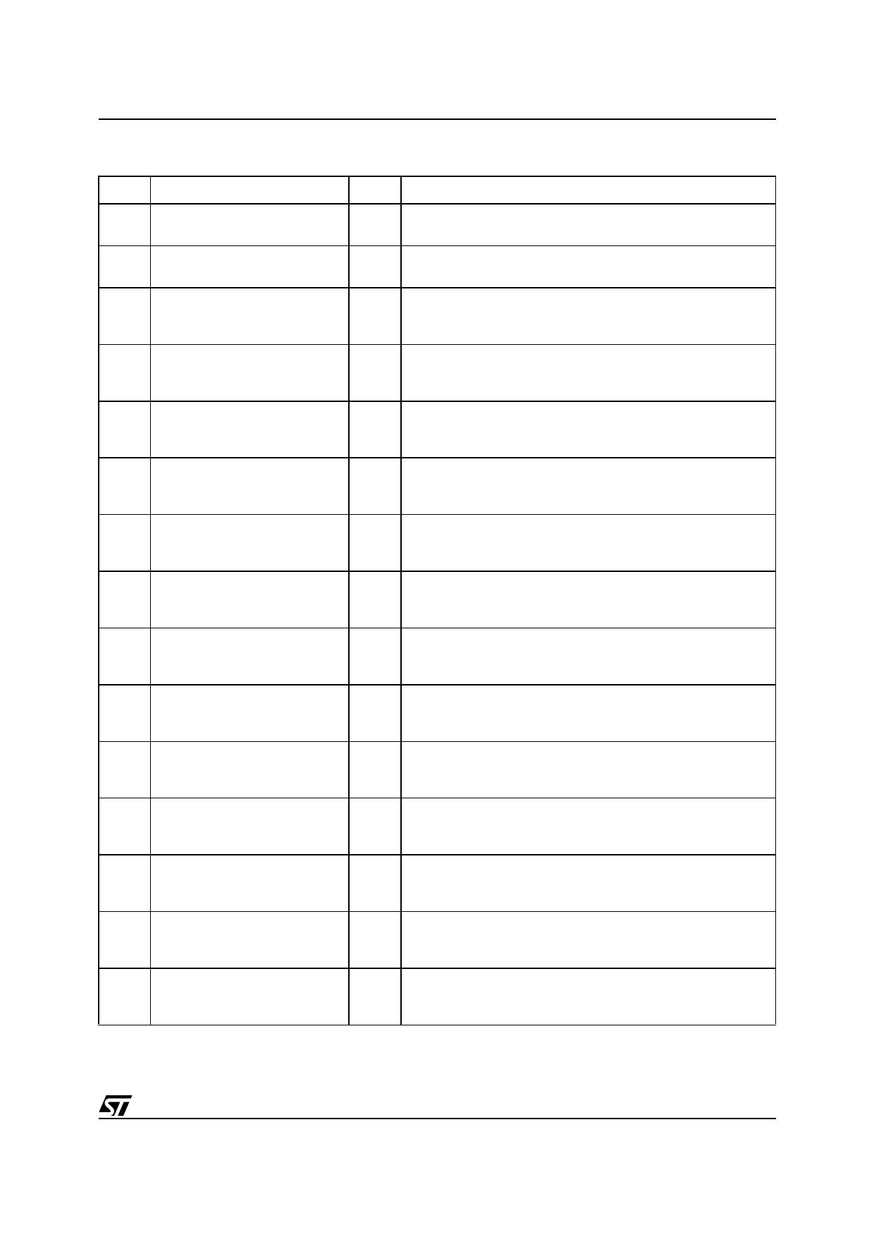
PIN DESCRIPTION (continued)
N°
Name
31 DSRA<5>
32 DSRA<4>
33 DSRA<3>
34 DSRA<2>
35 DSRA<1>
36 DSRA<0>
37 SRA<0>
38 SRA<1>
39 SRA<2>
40 SRA<3>
41 SRA<4>
42 SRA<5>
43 SRA<6>
44 SRA<7>
45 SRA<8>
TDA7500A
Type
Description
I/O DSP SRAM Data Lines<5> (Input/Output). When in SRAM
Mode this pin act as the EMI data line 5.
I/O DSP SRAM Data Lines<4> (Input/Output). When in SRAM
Mode this pin act as the EMI data line 4.
I/O DSP SRAM Data Lines<3> (Input/Output)/DSP DRAM Data
Line<3>(Input/Output). This pin act as the EMI data line 3 in
both SRAM Mode and DRAM Mode.
I/O DSP SRAM Data Lines<2> (Input/Output)/DSP DRAM Data
Line<2>(Input/Output). This pin act as the EMI data line 2 in
both SRAM Mode and DRAM Mode.
I/O DSP SRAM Data Lines<1> (Input/Output)/DSP DRAM Data
Line<1>(Input/Output). This pin act as the EMI data line 1 in
both SRAM Mode and DRAM Mode.
I/O DSP SRAM Data Lines<0> (Input/Output)/DSP DRAM Data
Line<0>(Input/Output). This pin act as the EMI data line 0 in
both SRAM Mode and DRAM Mode.
O DSP SRAM Address Line<0> (Output)/DSP DRAM Address
Line<0> (Output). This pin acts as the EMI address line 0 in both
SRAM Mode and DRAM Mode
O DSP SRAM Address Line<1> (Output)/DSP DRAM Address
Line<1> (Output). This pin acts as the EMI address line 1 in both
SRAM Mode and DRAM Mode
O DSP SRAM Address Line<2> (Output)/DSP DRAM Address
Line<2> (Output). This pin acts as the EMI address line 2 in both
SRAM Mode and DRAM Mode
O DSP SRAM Address Line<3> (Output)/DSP DRAM Address
Line<3> (Output). This pin acts as the EMI address line 3 in both
SRAM Mode and DRAM Mode
O DSP SRAM Address Line<4> (Output)/DSP DRAM Address
Line<4> (Output). This pin acts as the EMI address line 4 in both
SRAM Mode and DRAM Mode
O DSP SRAM Address Line<5> (Output)/DSP DRAM Address
Line<5> (Output). This pin acts as the EMI address line 5 in both
SRAM Mode and DRAM Mode
O DSP SRAM Address Line<6> (Output)/DSP DRAM Address
Line<6> (Output). This pin acts as the EMI address line 6 in both
SRAM Mode and DRAM Mode
O DSP SRAM Address Line<7> (Output)/DSP DRAM Address
Line<7> (Output). This pin acts as the EMI address line 7 in both
SRAM Mode and DRAM Mode
O DSP SRAM Address Line<8> (Output)/DSP DRAM Address
Line<8> (Output). This pin acts as the EMI address line 8 in both
SRAM Mode and DRAM Mode
5/40
Share Link: 