T4312816B-6S Ver la hoja de datos (PDF) - Taiwan Memory Technology
Número de pieza
componentes Descripción
fabricante
T4312816B-6S Datasheet PDF : 70 Pages
| |||
tm TE
CH
T4312816B
6 Write command
(RAS# = "H", CAS# = "L", WE# = "L", BAs = Bank, A10 = "L", A0-A8 = Column Address)
The Write command is used to write a burst of data on consecutive clock cycles from an active row in an
active bank. The bank must be active for at least tRCD(min.) before the Write command is issued. During write
bursts, the first valid data-in element will be registered coincident with the Write command. Subsequent data
elements will be registered on each successive positive clock edge (refer to the following figure). The DQs
remain with high-impedance at the end of the burst unless another command is initiated. The burst length and
burst sequence are determined by the mode register, which is already programmed. A full-page burst will
continue until terminated (at the end of the page it will wrap to column 0 and continue).
T0
T1
T2
T3
T4
T5
T6
T7
T8
CLK
COMMAND
NOP
WRITE A
NOP
NOP
NOP
NOP
NOP
NOP
NOP
DQ0 - DQ3
DIN A0
DIN A1
DIN A2
DIN A3
don't care
The first data element and the write
are registered on the same clock edge.
Extra data is masked.
Burst Write Operation (Burst Length = 4, CAS# Latency = 1, 2, 3)
A write burst without the auto precharge function may be interrupted by a subsequent Write,
BankPrecharge/PrechargeAll, or Read command before the end of the burst length. An interrupt coming from
Write command can occur on any clock cycle following the previous Write command (refer to the following
figure).
T0
T1
T2
T3
T4
T5
T6
T7
T8
CLK
COMMAND
NOP
WRITE A WRITE B
NOP
NOP
NOP
NOP
NOP
NOP
1 Clk Interval
DQ's
DIN A0
DIN B0
DIN B1
DIN B2
DIN B3
Write Interrupted by a Write (Burst Length = 4, CAS# Latency = 1, 2, 3)
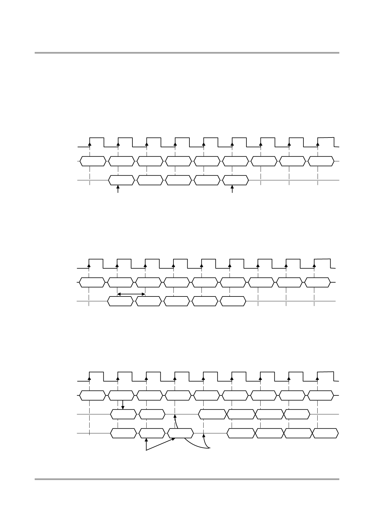
The Read command that interrupts a write burst without auto precharge function should be issued one
cycle after the clock edge in which the last data-in element is registered. In order to avoid data contention, input
data must be removed from the DQs at least one clock cycle before the first read data appears on the outputs
(refer to the following figure). Once the Read command is registered, the data inputs will be ignored and writes
will not be executed.
T0
T1
T2
T3
T4
T5
T6
T7
T8
CLK
COMMAND
NOP
WRITE A READ B
NOP
NOP
NOP
NOP
NOP
NOP
CAS# latency=2
tCK2, DQ's
DIN A0
don't care
DOUT B0
DOUT B1 DOUT B2 DOUT B3
CAS# latency=3
tCK3, DQ's
DIN A0
don't care don't care
DOUT B0
DOUT B1 DOUT B2 DOUT B3
Input data for the write is masked.
Input data must be removed from the DQ's at least one clock
cycle before the Read data appears on the outputs to avoid
data contention.
Write Interrupted by a Read (Burst Length = 4, CAS# Latency = 2, 3)
TM Technology Inc. reserves the right
P. 8
to change products or specifications without notice.
Publication Date: FEB. 2007
Revision: A
Share Link: 