SI4704-C40-GM Ver la hoja de datos (PDF) - Silicon Laboratories
Número de pieza
componentes Descripción
fabricante
SI4704-C40-GM Datasheet PDF : 36 Pages
| |||
Si4704/05-C40
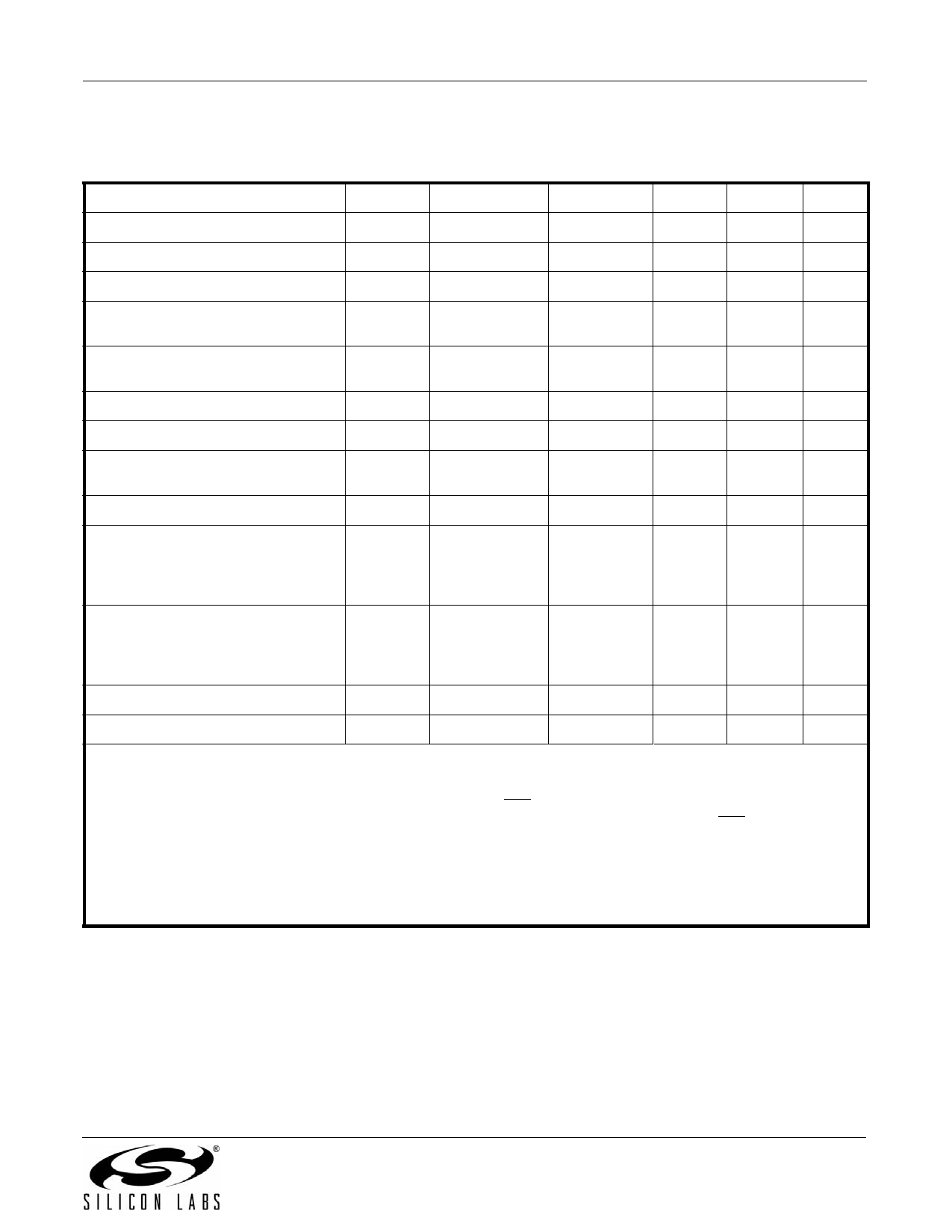
Table 5. 2-Wire Control Interface Characteristics1,2,3
(VDD = 2.7 to 5.5 V, VIO = 1.85 to 3.6 V, TA = –20 to 85 °C)
Parameter
SCLK Frequency
SCLK Low Time
SCLK High Time
SCLK Input to SDIO Setup
(START)
SCLK Input to SDIO Hold
(START)
SDIO Input to SCLK Setup
SDIO Input to SCLK Hold 4, 5
SCLK Input to SDIO Setup
(STOP)
STOP to START Time
SDIO Output Fall Time
Symbol Test Condition
Min
Typ
fSCL
tLOW
tHIGH
tSU:STA
0
—
1.3
—
0.6
—
0.6
—
tHD:STA
0.6
—
tSU:DAT
tHD:DAT
tSU:STO
100
—
0
—
0.6
—
tBUF
tf:OUT
1.3
—
—
20
+
0.1
--C-----b---
1pF
Max
Unit
400
kHz
—
µs
—
µs
—
µs
—
µs
—
ns
900
ns
—
µs
—
µs
250
ns
SDIO Input, SCLK Rise/Fall Time
tf:IN
tr:IN
—
20
+
0.1
--C-----b---
1pF
300
ns
SCLK, SDIO Capacitive Loading
Cb
—
—
50
pF
Input Filter Pulse Suppression
tSP
—
—
50
ns
Notes:
1. When VIO = 0 V, SCLK and SDIO are low impedance.
2. When selecting 2-wire mode, the user must ensure that a 2-wire start condition (falling edge of SDIO while SCLK is
high) does not occur within 300 ns before the rising edge of RST.
3. When selecting 2-wire mode, the user must ensure that SCLK is high during the rising edge of RST, and stays high
until after the first start condition.
4. The Si4704/05 delays SDIO by a minimum of 300 ns from the VIH threshold of SCLK to comply with the minimum
tHD:DAT specification.
5. The maximum tHD:DAT has only to be met when fSCL = 400 kHz. At frequencies below 400 KHz, tHD:DAT may be
violated as long as all other timing parameters are met.
Rev. 1.0
7
Share Link: 