SA8027W Ver la hoja de datos (PDF) - Philips Electronics
Número de pieza
componentes Descripción
fabricante
SA8027W
Philips Electronics
SA8027W Datasheet PDF : 22 Pages
| |||
Philips Semiconductors
2.5 GHz low voltage, low power
RF fractional-N/IF integer frequency synthesizer
Product data
SA8027
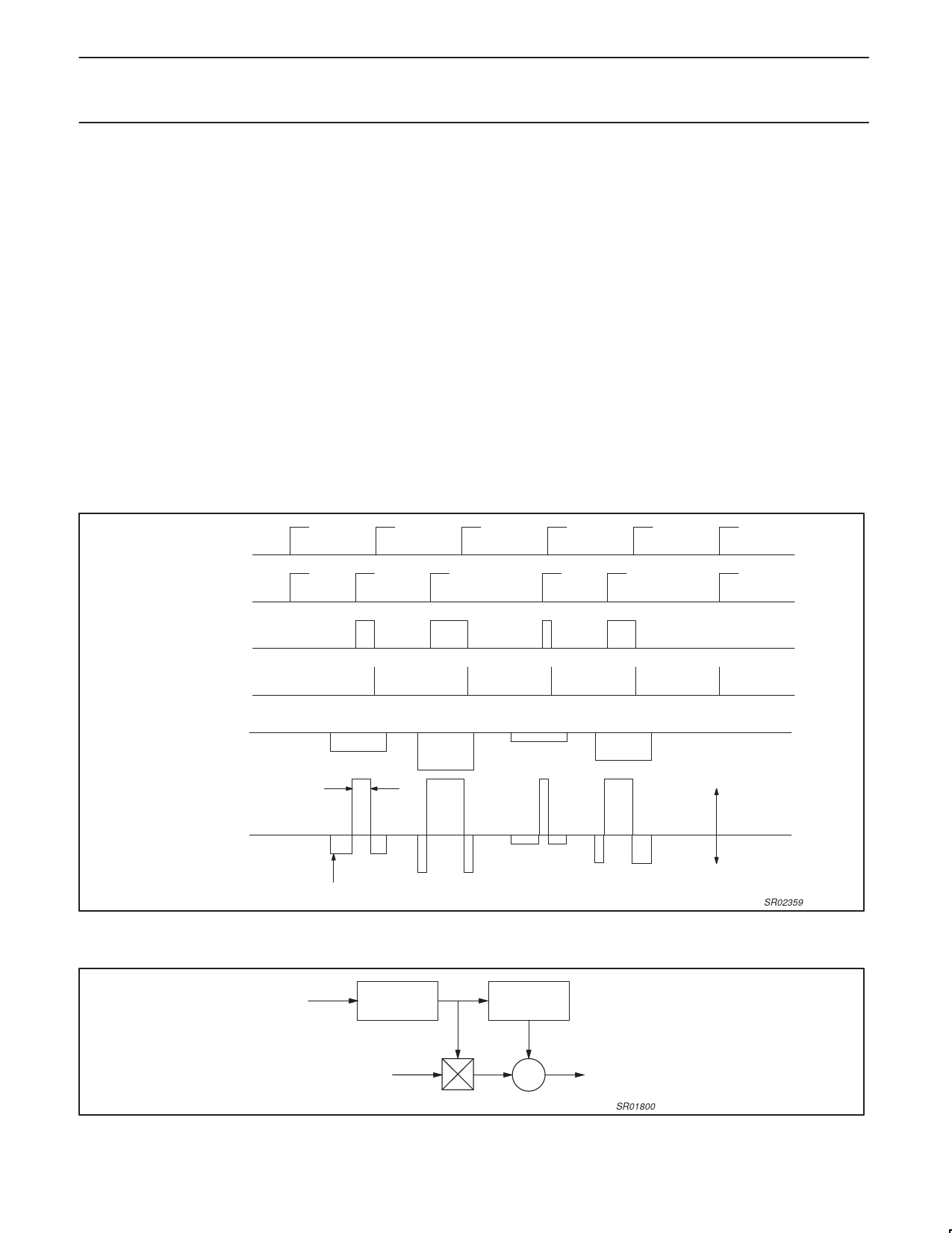
1.5 Main Output Charge Pumps and Fractional
Compensation Currents (see Figure 8)
The main charge pumps on pins PHP and PHI are driven by the
main phase detector and the charge pump current values are
determined by the current at pin RSET in conjunction with bits CP0,
CP1 in the C-word (see Table 1). The main charge pumps will enter
speed up mode after the A-word is set and strobe goes High. When
strobe goes Low, charge pump will exit speed up mode. The
fractional compensation is derived from the current at RSET, the
contents of the fractional accumulator (FRD) and by the program
value of the FDAC. The timing for the fractional compensation is
derived from the main divider.
1.6 Principle of Fractional Compensation
The fractional compensation is designed into the circuit as a means
of reducing or eliminating fractional spurs that are caused by the
fractional phase ripple of the main divider. If ICOMP is the
compensation current and IPUMP is the pump current, then for each
charge pump:
IPUMP_TOTAL = IPUMP + ICOMP.
The compensation is done by sourcing a small current, ICOMP, see
Figure 9, that is proportional to the fractional error phase. For proper
fractional compensation, the area of the fractional compensation
current pulse must be equal to the area of the fractional charge
pump ripple. The width of the fractional compensation pulse is fixed
to 128 VCO cycles, the amplitude is proportional to the fractional
accumulator value and is adjusted by FDAC values (bits FC7–0 in
the B-word). The fractional compensation current is derived from the
main charge pump in that it follows all the current scaling through
external resistor setting, RSET, programming or speed-up operation.
For a given charge pump,
ICOMP = ( IPUMP / 128 ) * ( FDAC / 5*128) * FRD
FRD is the fractional accumulator value and is automatically
updated.
The theoretical values for FDAC are: 128 for FMOD = 1 (modulo 5)
and 80 for FMOD = 0 (modulo 8).
REFERENCE R
MAIN M DIVIDE RATIO
N
N
N+1
N
N+1
CHARGE PUMP OUTPUT
ACCUMULATOR VALUE (FRD)
FRACTIONAL COMPENSATION
CURRENT (ICOMP)
2
4
1
3
0
PULSE
WIDTH
MODULATION
mA
IPUMP–TOTAL
µA
PULSE LEVEL
MODULATION
GRAPHS NOT TO SCALE.
NOTE: For a proper fractional compensation, the area of the fractional compensation current pulse must be equal to the area of the charge pump output.
Figure 8. Waveforms for NF = 2 Modulo 5 → fraction = 2/5
SR02359
fRF
MAIN DIVIDER
FRACTIONAL
ACCUMULATOR
ICOMP
fREF
Σ IPUMP
LOOP FILTER
& VCO
Figure 9. Current Injection Concept
SR01800
2001 Aug 21
10
Share Link: 