PSD802F2-15MI Ver la hoja de datos (PDF) - STMicroelectronics
Número de pieza
componentes Descripción
fabricante
PSD802F2-15MI Datasheet PDF : 94 Pages
| |||
Preliminary Information
PSD9XX Family
Pin Capacitance
TA = 25 °C, f = 1 MHz
Symbol
Parameter 1
Conditions Typical2 Max Unit
CIN
Capacitance (for input pins only)
VIN = 0 V
4
6 pF
COUT
Capacitance (for input/output pins)
VOUT = 0 V
8
12 pF
CVPP
Capacitance (for CNTL2/VPP)
VPP = 0 V
18
25 pF
NOTES: 1. These parameters are only sampled and are not 100% tested.
2. Typical values are for TA = 25°C and nominal supply voltages.
Figure 33.
AC Testing
Input/Output
Waveform
3.0V
0V
TEST POINT
1.5V
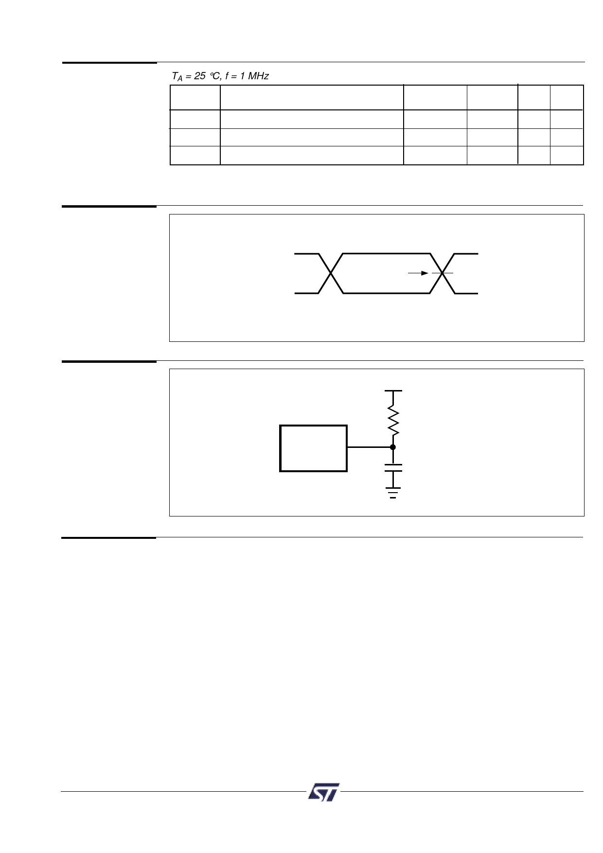
Figure 34.
AC Testing
Load Circuit
DEVICE
UNDER TEST
2.01 V
195 Ω
CL = 30 pF
(INCLUDING
SCOPE AND JIG
CAPACITANCE)
Programming
Upon delivery from ST, the PSD9XX device has all bits in the PLDs and
memories in the “1” or high state. The configuration bits are in the “0” or low state. The
code, configuration, and PLDs logic are loaded through the procedure of programming.
Information for programming the device is available directly from ST. Please contact your
local sales representative. (See the last page.)
81
Share Link: 