NCP3163PWR2G Ver la hoja de datos (PDF) - ON Semiconductor
Número de pieza
componentes Descripción
fabricante
NCP3163PWR2G Datasheet PDF : 20 Pages
| |||
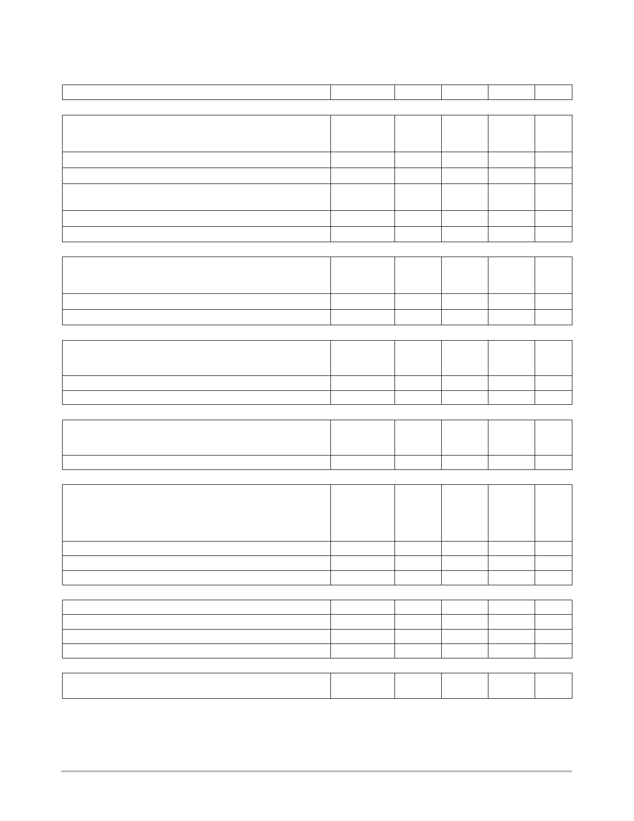
NCP3163, NCV3163
ELECTRICAL CHARACTERISTICS (VCC = 15 V, Pin 16 = VCC, CT = 270 pF, RT = 15 kW, for typical values TA = 25°C, for min/max
values TA is the operating ambient temperature range that applies (Note 7), unless otherwise noted.)
Characteristic
Symbol
Min
Typ
Max
Unit
OSCILLATOR
Frequency
TA = 25°C, VCC = 15 V
Total Variation over VCC = 2.5 V to 40 V and Temperature
fOSC
kHz
225
250
275
212
250
288
Charge Current
Ichg
−
225
−
mA
Discharge Current
Idischg
−
25
−
mA
Charge to Discharge Current Ratio
NCP3163 Ichg/Idischg
8.0
NCV3163
7.0
9.0
10.5
−
9.0
10.5
Sawtooth Peak Voltage
Sawtooth Valley Voltage
FEEDBACK COMPARATOR 1
Threshold Voltage
TA = 25°C
Total Variation over VCC = 2.5 V to 40 V and Temperature
Threshold Voltage − Line Regulation (VCC = 2.5 V to 40 V, TA = 25°C)
Input Bias Current (VFB1 = 5.05 V)
FEEDBACK COMPARATOR 2
Threshold Voltage
TA = 25°C, VCC = 15 V
Total Variation over VCC = 2.5 V to 40 V and Temperature
Threshold Voltage − Line Regulation (VCC = 2.5 V to 40 V, TA = 25°C)
Input Bias Current (VFB2 = 1.25 V)
CURRENT LIMIT COMPARATOR
Threshold Voltage
TA = 25°C
Total Variation over VCC = 2.5 V to 40 V, and Temperature
Input Bias Current (VIpk (Sense) = 15 V)
DRIVER AND OUTPUT SWITCH (Note 6)
Saturation Voltage (ISW = 2.5 A, Pins 14, 15 grounded)
Non−Darlington (RPin 9 = 110 W to VCC, ISW/IDRV ≈ 20)
Darlington Connection (Pins 9, 10, 11 connected)
NCP3163
NCV3163
NCP3163
NCV3163
VOSC(P)
VOSC(V)
Vth(FB1)
REGline(FB1)
IIB(FB1)
Vth(FB2)
REGline(FB1)
IIB(FB2)
Vth(Sense)
IIB(Sense)
VCE(sat)
−
−
4.9
4.85
−
−
1.225
1.213
−
− 0.4
−
225
−
−
−
−
−
1.25
0.55
5.05
−
0.008
100
1.25
−
0.008
−
250
−
1.0
0.6
0.6
1.0
1.0
−
V
−
V
V
5.2
5.25
0.03
%/V
200
mA
V
1.275
1.287
0.03
%/V
0.4
mA
mV
−
270
20
mA
V
1.0
1.5
1.4
1.5
Collector Off−State Leakage Current (VCE = 40 V)
Bootstrap Input Current Source (VBS = VCC + 5.0 V)
Bootstrap Input Zener Clamp Voltage (IZ = 25 mA)
IC(off)
−
0.02
100
mA
Isource(DRV)
0.5
2.0
4.0
mA
VZ
VCC + 6.0 VCC + 7.0 VCC + 9.0
V
LOW VOLTAGE INDICATOR
Input Threshold (VFB2 Increasing)
Input Hysteresis (VFB2 Decreasing)
Output Sink Saturation Voltage (Isink = 2.0 mA)
Output Off−State Leakage Current (VOH = 15 V)
Vth
VH
VOL(LVI)
IOH
1.07
1.125
1.18
V
−
15
−
mV
−
0.15
0.4
V
−
0.01
5.0
mA
TOTAL DEVICE
Standby Supply Current (VCC = 2.5 V to 40 V, Pin 8 = VCC,
Pins 6, 14, 15 = GND, remaining pins open)
ICC
−
6.0
10
mA
5. Maximum package power dissipation limits must be observed.
6. Low duty cycle pulse techniques are used during test to maintain junction temperature as close to ambient as possible.
7. Tlow = 0°C for NCP3163
= − 40°C for NCP3163B
Thigh = + 70°C for NCP3163
= + 85°C for NCP3163B
= − 40°C for NCV3163
= + 125°C for NCV3163
http://onsemi.com
4
Share Link: 