AD9070(RevB) Ver la hoja de datos (PDF) - Analog Devices
Número de pieza
componentes Descripción
fabricante
AD9070 Datasheet PDF : 16 Pages
| |||
AD9070
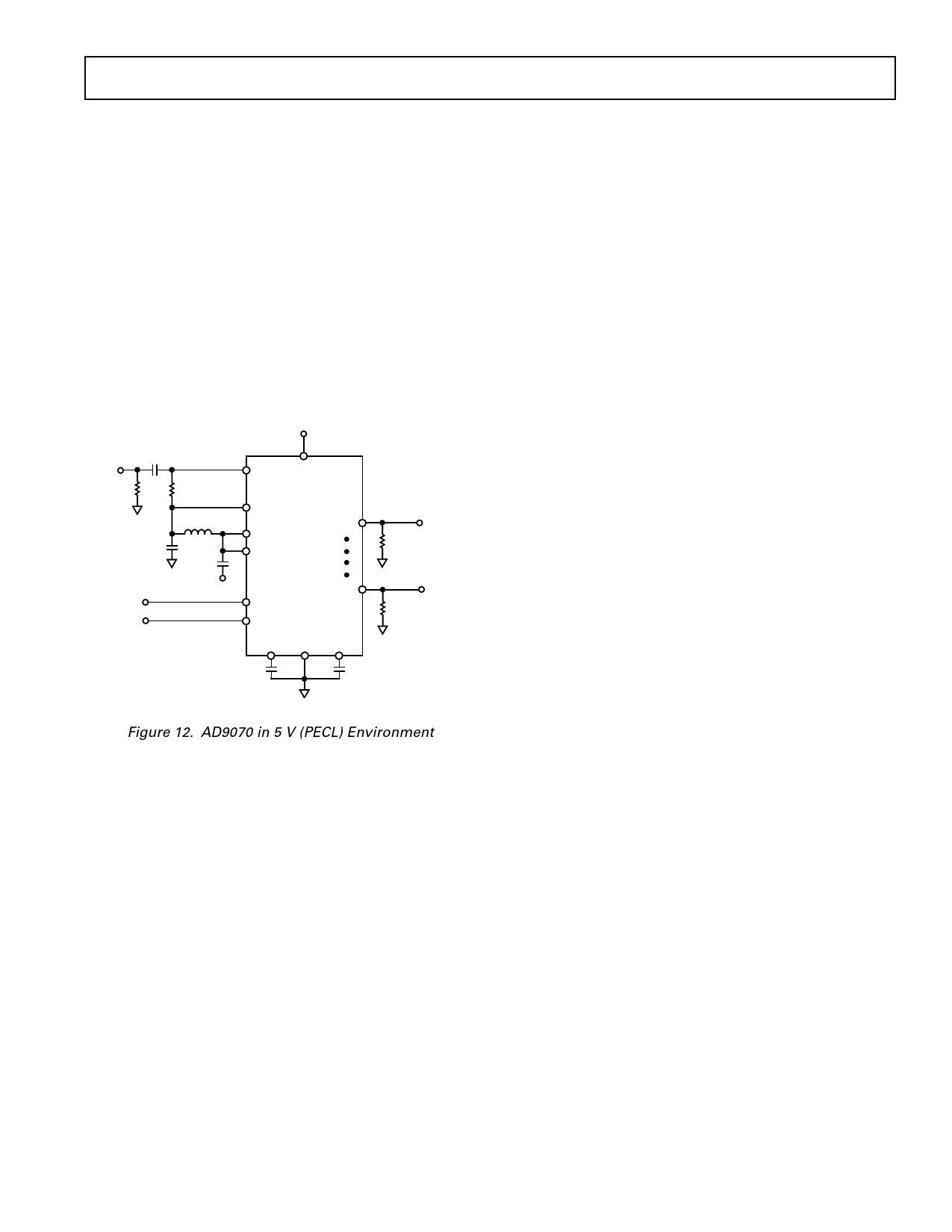
+5 V Operation
The AD9070 may be operated above ground, with a single +5 V
power supply. All power supply ground pins are connected to
+5 V, and VEE pins are connected to ground (Figure 22). Care
must be taken in connecting signals and determining bypass rails.
The reference voltage (REF OUT) is still generated with respect
to the positive rail, which is now +5 V. It is nominally +2.5 V,
but its voltage with respect to ground will vary directly with
changes in the power supply voltage (for example, if the power
supply goes to +5.1 V, the reference becomes +2.6 V). The
reference input is likewise processed with respect to +5 V. This
dictates that these pins be bypassed to +5 V as well. However,
the COMP and REF BYPASS pins must continue to be
bypassed to the most negative supply, which is now ground. The
AIN input must still be connected or bypassed to the ground
reference of the input signal.
Package Options
The AD9070 is available in two packages. The BR package is a
standard 28-lead Small Outline IC (SOIC). The DIP package is
a ceramic Dual-in-Line Hybrid. The SOIC is offered in a commer-
cial grade, and specified over the industrial (–40°C to +85°C)
temperature range. The DIP is a full MIL-PRF-38534 QML
version that operates from (–55°C to +125°C).
The SOIC version includes the on-chip voltage reference,
whereas the DIP does not. The DIP, however, provides the
Overrange (OR) output, and includes reference and power
supply bypassing, along with an internal compensation capacitor.
Equivalent performance may be obtained with either part
though, due to the internal bypassing, the DIP is not as sensitive
to board layout and parasitics.
+5V
VIN
1Vp-p
0.1F
RT
500⍀
0.1F
10H
0.1F
AIN
GND
AD9070
AIN
(MSB) D9
VREF OUT
VREF IN
D9
510⍀
(OR 100⍀ TO +3V)
ENCODE
ENCODE
+5V
(LSB) D0
ENCODE
ENCODE
REF
COMP VEE BYPASS
D0
510⍀
(OR 100⍀ TO +3V)
0.1F
0.1F
Figure 22. AD9070 in +5 V (PECL) Environment
REV. B
–11–
Share Link: 