N74F827N(2004) Ver la hoja de datos (PDF) - Philips Electronics
Número de pieza
componentes Descripción
fabricante
N74F827N Datasheet PDF : 11 Pages
| |||
Philips Semiconductors
10-bit buffer/line driver, non-inverting (3-State)
Product data
74F827
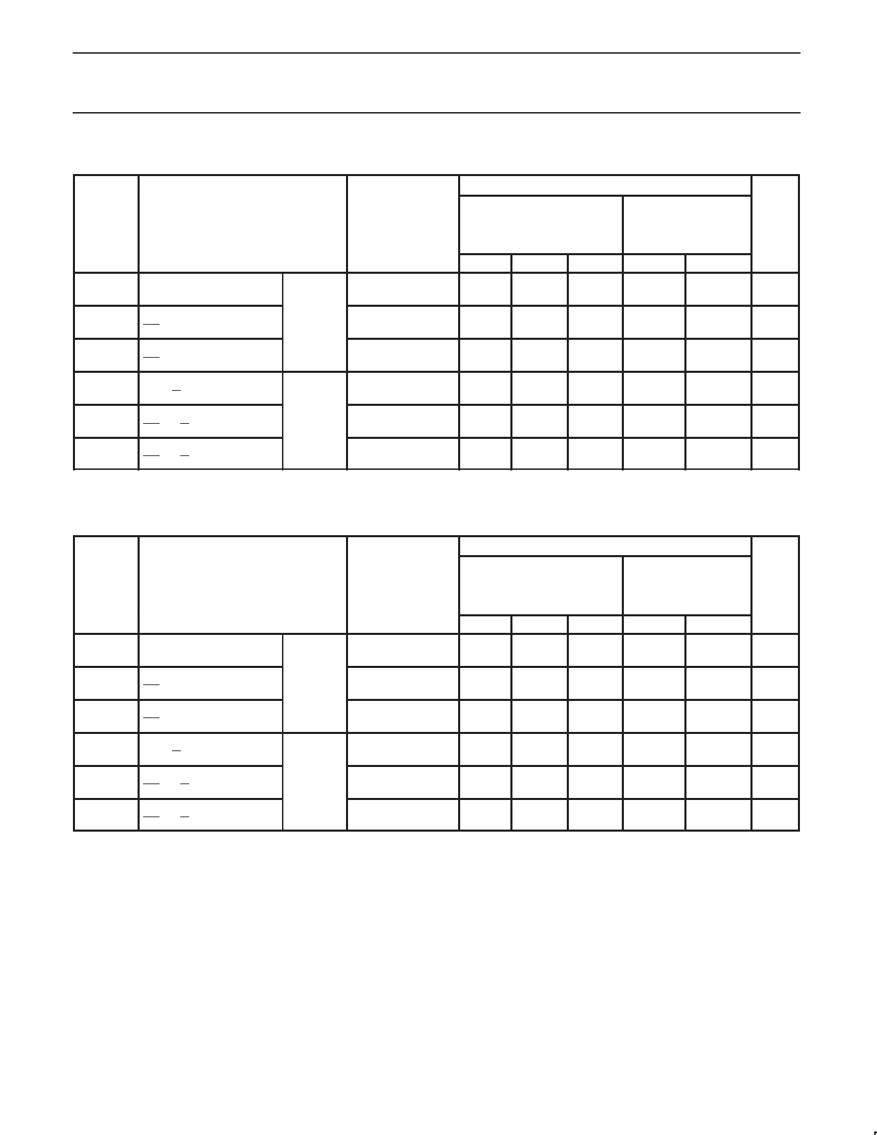
AC CHARACTERISTICS
SYMBOL
PARAMETER
tPLH
tPHL
tPZH
tPZL
tPHZ
tPLZ
Propagation delay
Dn to Qn
Output enable time
OEn to Qn
Output disable time
OEn to Qn
CONDITIONS
Waveform 1
Waveform 2
Waveform 3
Waveform 2
Waveform 3
LIMITS
Tamb = +25 °C
VCC = 5 V
CL = 50 pF; RL = 500 Ω
Tamb = 0 °C to +70 °C
VCC = 5 V ± 10%
CL = 50 pF; RL = 500 Ω
Min
Typ
Max
Min
Max
2.0
5.5
8.5
2.0
9.0
2.0
4.5
8.5
2.0
9.0
5.0
8.0
12.0
4.5
14.0
4.0
6.0
10.5
4.0
11.5
2.5
5.0
8.0
2.0
8.5
2.5
5.0
8.0
2.0
8.5
UNIT
ns
ns
ns
AC CHARACTERISTICS
For 1 Output switching with CL = 300 pF and RL = 500 Ω load
SYMBOL
PARAMETER
CONDITIONS
tPLH
tPHL
tPZH
tPZL
tPHZ
tPLZ
Propagation delay
Dn to Qn
Output enable time
OEn to Qn
Output disable time
OEn to Qn
Waveform 1
Waveform 2
Waveform 3
Waveform 2
Waveform 3
LIMITS
Tamb = +25 °C
VCC = 5 V
CL = 300 pF; RL = 500 Ω
Tamb = 0 °C to +70 °C
VCC = 5 V ± 10%
CL = 300 pF; RL = 500 Ω
MIN
Typ
Max
MIN
Max
–
9.5
13.0
–
14.0
–
7.5
10.0
–
11.0
–
15.0 20.0
–
21.0
–
9.5
13.0
–
14.0
–
15.0 19.0
–
20.0
–
9.5
13.5
–
14.0
UNIT
ns
ns
ns
AC CHARACTERISTICS
For 10 Outputs switching with CL = 300 pF and RL = 500 Ω load
SYMBOL
PARAMETER
CONDITIONS
tPLH
tPHL
tPZH
tPZL
tPHZ
tPLZ
Propagation delay
Dn to Qn
Output enable time
OEn to Qn
Output disable time
OEn to Qn
Waveform 1
Waveform 2
Waveform 3
Waveform 2
Waveform 3
LIMITS
Tamb = +25 °C
VCC = 5 V
CL = 300 pF; RL = 500 Ω
Tamb = 0 °C to +70 °C
VCC = 5 V ± 10%
CL = 300 pF; RL = 500 Ω
MIN
Typ
Max
MIN
Max
–
12.0 16.0
–
17.0
–
14.0 17.0
–
18.0
–
15.0 20.0
–
21.0
–
17.0 21.0
–
21.5
–
15.0 19.0
–
20.0
–
12.5 15.5
–
16.0
UNIT
ns
ns
ns
2004 Jan 21
6
Share Link: 