MM74HC4538MX Ver la hoja de datos (PDF) - Fairchild Semiconductor
Número de pieza
componentes Descripción
fabricante
MM74HC4538MX Datasheet PDF : 10 Pages
| |||
Circuit Operation (Continued)
toggle, taking the Q output of the HC4538 to a LOW State
(#19), and completing the time-out cycle.
RESET OPERATION
A low voltage applied to the Reset pin always forces the Q
output of the HC4538 to a LOW State.
The timing diagram illustrates the case in which reset
occurs (#20) while CX is charging up toward the reference
voltage of the upper reference circuit (#21). When a reset
occurs, the output of the reset latch goes LOW (#22), turn-
ing ON transistor M1. Thus CX is allowed to quickly charge
up to VCC (#23) to await the next trigger signal.
Recovery time is the required delay after reset goes inac-
tive to a new trigger rising edge. On the diagram it is shown
as (#26) to (#27).
RETRIGGER OPERATION
In the retriggerable mode, the HC4538 may be retriggered
during timing out of the output pulse at any time after the
trigger-control circuit flip-flop has been reset (#24).
Because the trigger-control circuit flip-flop resets shortly
after CX has discharged to the reference voltage of the
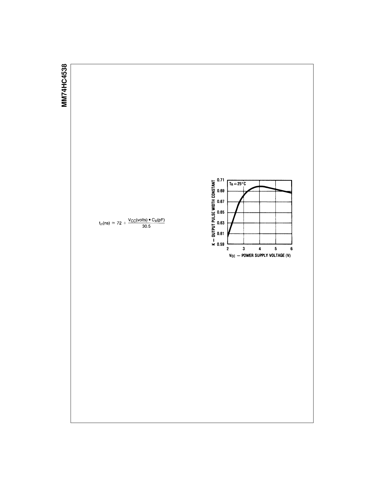
lower reference circuit (#25), the minimum retrigger time, trr
is a function of internal propagation delays and the dis-
charge time of CX:
device is powered down, the capacitor may discharge from
VCC through the input protection diodes at pin 2 or pin 14.
Current through the protection diodes must be limited to 30
mA; therefore, the turn-off time of the VCC power supply
must not be faster than t = VCC•CX/(30 mA). For example, if
VCC = 5V and CX = 15 µF, the VCC supply must turn OFF
no faster than t = (15V)•(15 µF)/30 mA = 2.5 ms. This is
usually not a problem because power supplies are heavily
filtered and cannot discharge at this rate.
When a more rapid decrease of VCC to zero volts occurs,
the MM74HC4538 may sustain damage. To avoid this pos-
sibility, use an external clamping diode, DX, connected
from VCC to the CX pin.
SET UP RECOMMENDATIONS
Minimum RX = 1 kΩ
Minimum CX = 0 pF.
at room temperature
POWER-DOWN CONSIDERATIONS
Large values of CX may cause problems when powering
down the MM74HC4538 because of the amount of energy
stored in the capacitor. When a system containing this
www.fairchildsemi.com
4
Share Link: 