MM74C905N Ver la hoja de datos (PDF) - Fairchild Semiconductor
Número de pieza
componentes Descripción
fabricante
MM74C905N Datasheet PDF : 8 Pages
| |||
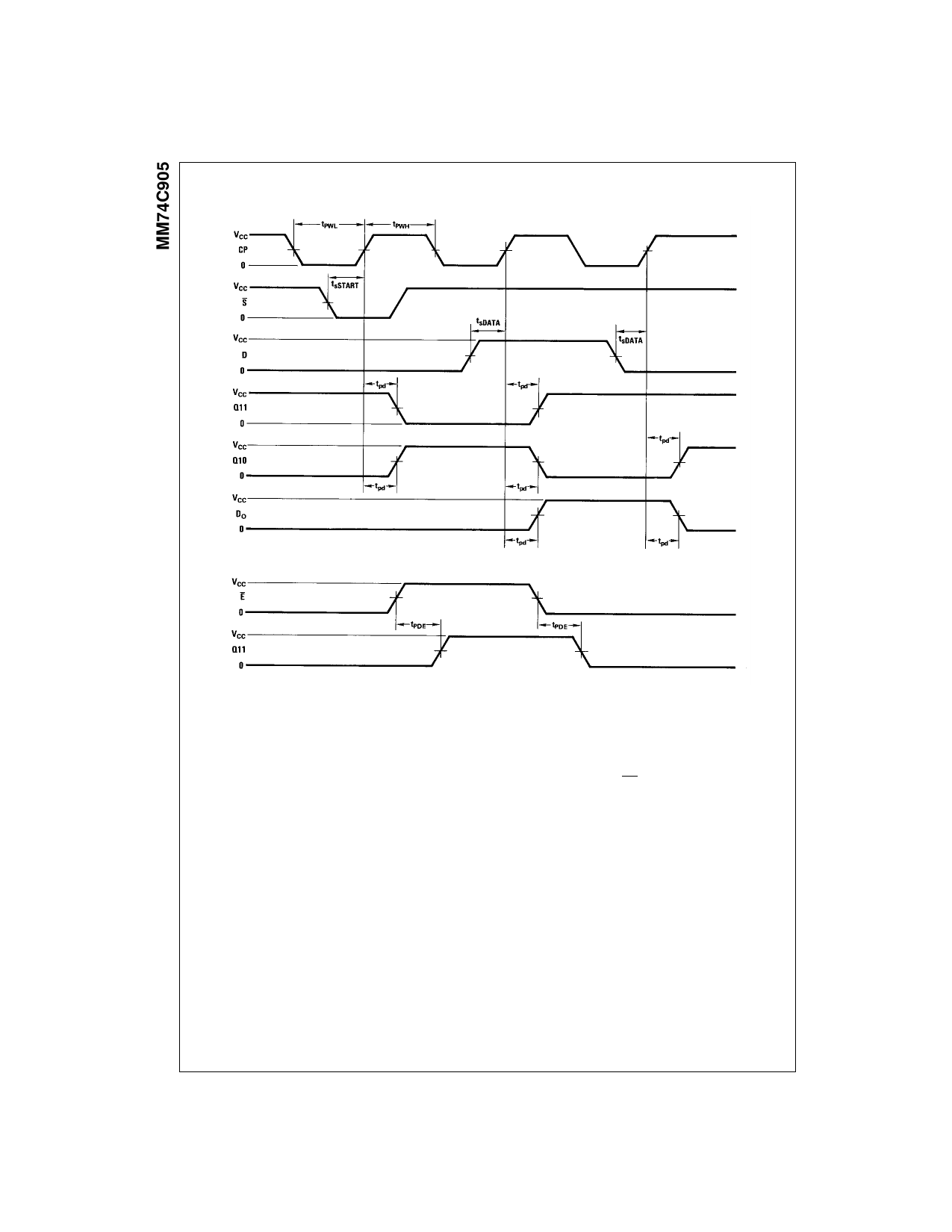
Switching Time Waveforms
USER NOTES FOR A/D CONVERSION
The register can be used with either current switches that
require a low voltage level to turn the switch ON or current
switches that require a high voltage level to turn the switch
ON. If current switches are used which turn ON with a low
logic level, the resulting digit output from the register is
active low. That is, a logic “1” is represented as a low volt-
age level. If current switches are used which turn ON with a
high logic level, the resulting digit output is active high. A
logic “1” is represented as a high voltage level.
For a maximum error of ±½ LSB, the comparator must be
biased. If current switches that require a high voltage level
to turn ON are used, the comparator should be biased +½
LSB and if the current switches require a low logic level to
turn ON, then the comparator must be biased −½ LSB.
The register can be used to perform 2's complement con-
version by offsetting the comparator one half full range +½
LSB and using the complement of the MSB Q11 as the sign
bit.
If the register is truncated and operated in the continuous
conversion mode, a lock-up condition may occur on power-
ON. This situation can be overcome by making the START
input the “OR” function of CC and the appropriate register
output.
The register, by suitable selection of register ladder net-
work, can be used to perform either binary or BCD conver-
sion.
The register outputs can drive the 10 bits or less with 50k/
100k R/2R ladder network directly for VCC = 10V or higher.
In order to drive the 12-bit 50k/100k ladder network and
have the ±½ LSB resolution, the MM74C902 or
MM74C904 is used as buffers, three buffers for MSB
(Q11), two buffers for Q10, and one buffer for Q9.
www.fairchildsemi.com
6
Share Link: 