MC14538BDW Ver la hoja de datos (PDF) - Motorola => Freescale
Número de pieza
componentes Descripción
fabricante
MC14538BDW Datasheet PDF : 10 Pages
| |||
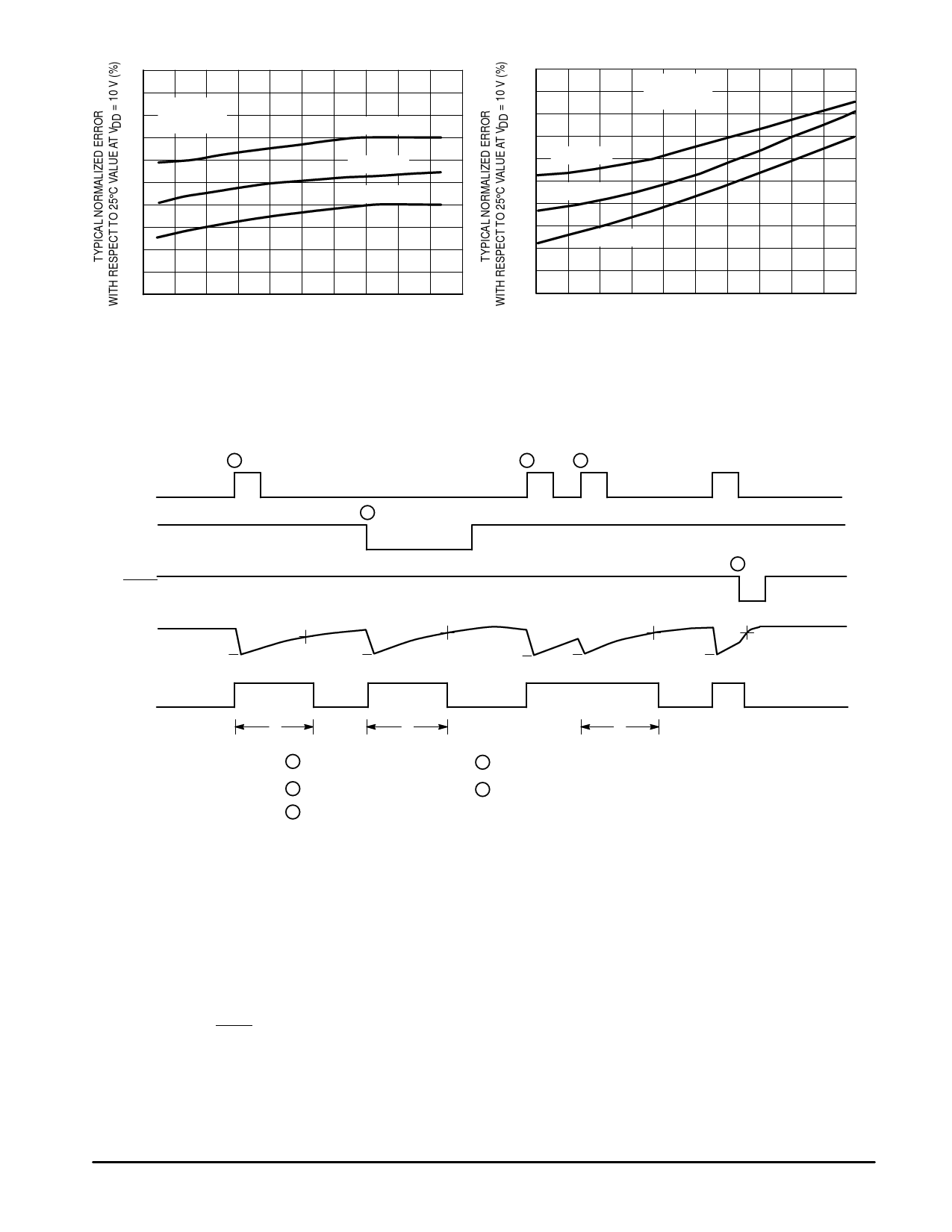
RX = 100 kΩ
CX = 0.1 µF
2
1
0
–1
–2
VDD = 15 V
VDD = 10 V
VDD = 5 V
RX = 100 kΩ
CX = .002 µF
3.0
2.0
1.0 VDD = 15 V
0
VDD = 10 V
– 1.0
– 2.0
– 3.0
VDD = 5.0 V
– 60 – 40 – 20 0 20 40 60 80 100 120 140
TA, AMBIENT TEMPERATURE (°C)
Figure 8. Typical Error of Pulse Width
Equation versus Temperature
– 60 – 40 – 20 0 20 40 60 80 100 120 140
TA, AMBIENT TEMPERATURE (°C)
Figure 9. Typical Error of Pulse Width
Equation versus Temperature
A
B
RESET
CX/RX
Q
THEORY OF OPERATION
1
3
4
2
5
Vref 1
Vref 2
Vref 1
Vref 2
Vref 1
Vref 2
Vref 2
Vref 1
T
T
T
1 Positive edge trigger
2 Negative edge trigger
3 Positive edge trigger
4 Positive edge re–trigger (pulse lengthening)
5 Positive edge re–trigger (pulse lengthening)
Figure 10. Timing Operation
TRIGGER OPERATION
The block diagram of the MC14538B is shown in Figure 1,
with circuit operation following.
As shown in Figure 1 and 10, before an input trigger
occurs, the monostable is in the quiescent state with the Q
output low, and the timing capacitor CX completely charged
to VDD. When the trigger input A goes from VSS to VDD
(while inputs B and Reset are held to VDD) a valid trigger is
recognized, which turns on comparator C1 and N–channel
transistor N1 . At the same time the output latch is set. With
transistor N1 on, the capacitor CX rapidly discharges toward
VSS until Vref1 is reached. At this point the output of
comparator C1 changes state and transistor N1 turns off.
Comparator C1 then turns off while at the same time
MC14538B
6
comparator C2 turns on. With transistor N1 off, the capacitor
CX begins to charge through the timing resistor, RX, toward
VDD. When the voltage across CX equals Vref 2, comparator
C2 changes state, causing the output latch to reset (Q goes
low) while at the same time disabling comparator C2 . This
ends at the timing cycle with the monostable in the quiescent
state, waiting for the next trigger.
In the quiescent state, CX is fully charged to VDD causing
the current through resistor RX to be zero. Both comparators
are “off” with total device current due only to reverse junction
leakages. An added feature of the MC14538B is that the out-
put latch is set via the input trigger without regard to the
capacitor voltage. Thus, propagation delay from trigger to Q
is independent of the value of CX, RX, or the duty cycle of the
input waveform.
MOTOROLA CMOS LOGIC DATA
Share Link: 