MAX44260_V4 Ver la hoja de datos (PDF) - Maxim Integrated
Número de pieza
componentes Descripción
fabricante
MAX44260_V4 Datasheet PDF : 16 Pages
| |||
MAX44260/MAX44261
1.8V 15MHz Low-Offset,
Low-Power, Rail-to-Rail I/O Op Amps
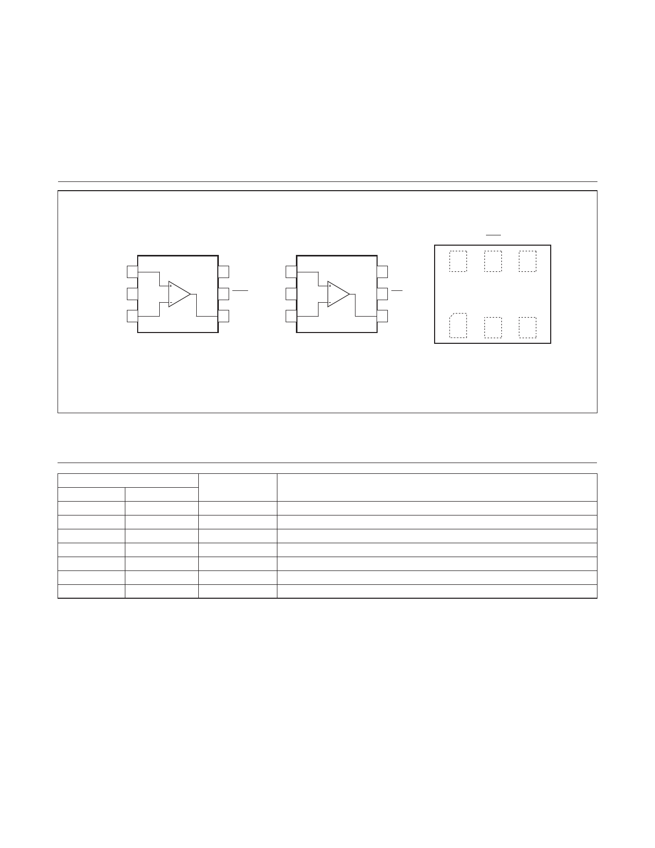
Pin Configurations
TOP VIEW
+
IN+ 1
VSS 2
IN- 3
MAX44260
NOT TO SCALE
+
6 VDD
IN+ 1
5 SHDN
VSS 2
4 OUT
IN- 3
SC70
MAX44261 6 VDD
5 CAL
4 OUT
SC70
VDD
SHDN
OUT
6
5
4
MAX44260
1
2
3
+
IN+
VSS
IN-
Thin µDFN
(Ultra-Thin LGA)
PIN
MAX44260
MAX44261
1
1
2
2
3
3
4
4
—
5
5
—
6
6
Pin Description
NAME
IN+
VSS
IN-
OUT
CAL
SHDN
VDD
FUNCTION
Positive Input
Negative Power Supply. Bypass with a 0.1FF capacitor to ground.
Negative Input
Output
Active-Low Calibrate Input
Active-Low Shutdown
Positive Power Supply. Bypass with a 0.1FF capacitor to ground.
9
Share Link: 