M28F201-70XN1 Ver la hoja de datos (PDF) - STMicroelectronics
Número de pieza
componentes Descripción
fabricante
M28F201-70XN1 Datasheet PDF : 21 Pages
| |||
M28F201
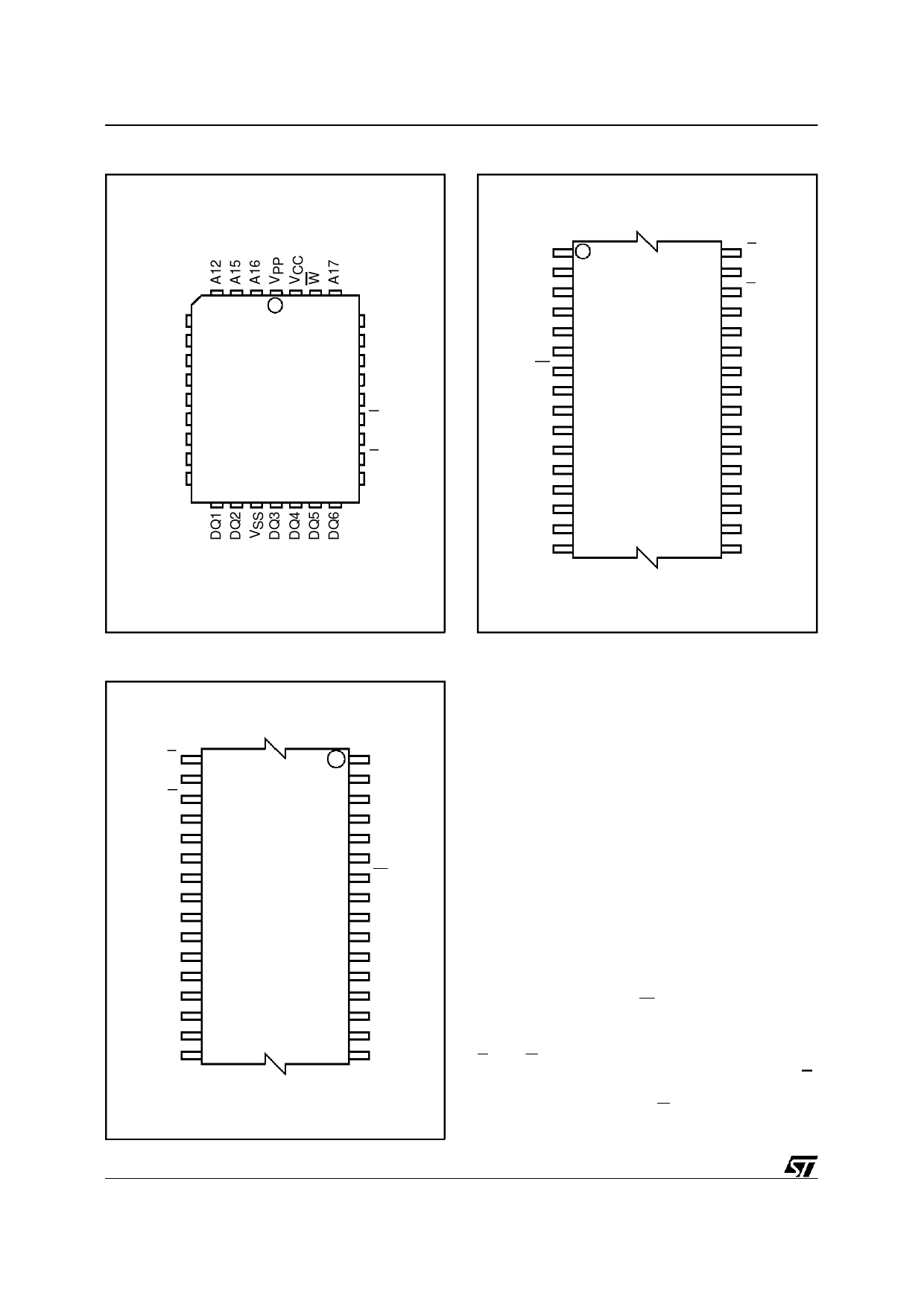
Figure 2A. LCC Pin Connections
Figure 2B. TSOP Pin Connections
A7
A6
A5
A4
A3 9
A2
A1
A0
DQ0
1 32
M28F201
17
A14
A13
A8
A9
25 A11
G
A10
E
DQ7
AI00638C
A11
A9
A8
A13
A14
A17
W
VCC
VPP
A16
A15
A12
A7
A6
A5
A4
1
32
8 M28F201 25
9 (Normal) 24
16
17
G
A10
E
DQ7
DQ6
DQ5
DQ4
DQ3
VSS
DQ2
DQ1
DQ0
A0
A1
A2
A3
AI00639C
Figure 2C. TSOP Reverse Pin Connections
G
A10
E
DQ7
DQ6
DQ5
DQ4
DQ3
VSS
DQ2
DQ1
DQ0
A0
A1
A2
A3
1
32 A11
A9
A8
A13
A14
A17
W
8 M28F201 25 VCC
9 (Reverse) 24 VPP
A16
A15
A12
A7
A6
A5
16
17 A4
AI00640D
2/21
DEVICE OPERATION
The M28F201 FLASH Memory product employs a
technology similar to a 2 Megabit EPROM but add
to the device functionality by providing electrical
erasure and programming. These functions are
managed by a command register. The functions
that are addressed via the command register de-
pend on the voltage applied to the VPP, program
voltage, input. When VPP is less than or equal to
6.5V, the command register is disabled and the
M28F201 functions as a read only memory provid-
ing operating modes similar to an EPROM (Read,
Output Disable, Electronic Signature Read and
Standby). When VPP is raised to 12V the command
register is enabled and this provides, in addition,
Erase and Program operations.
READ ONLY MODES, VPP ≤ 6.5V
For all Read Only Modes, except Standby Mode,
the Write Enable input W should be High. In the
Standby Mode this input is ’don’t care’.
Read Mode. The M28F201 has two enable inputs,
E and G, both of which must be Low in order to
output data from the memory. The Chip Enable (E)
is the power control and should be used for device
selection. Output Enable (G) is the output control
and should be used to gate data on to the output,
independantof the device selection.
Share Link: 