IDT8535-01 Ver la hoja de datos (PDF) - Integrated Device Technology
Número de pieza
componentes Descripción
fabricante
IDT8535-01 Datasheet PDF : 11 Pages
| |||
IDT8535-01
LOW SKEW, 1-TO-4 LVCMOS-TO-3.3V LVPECL
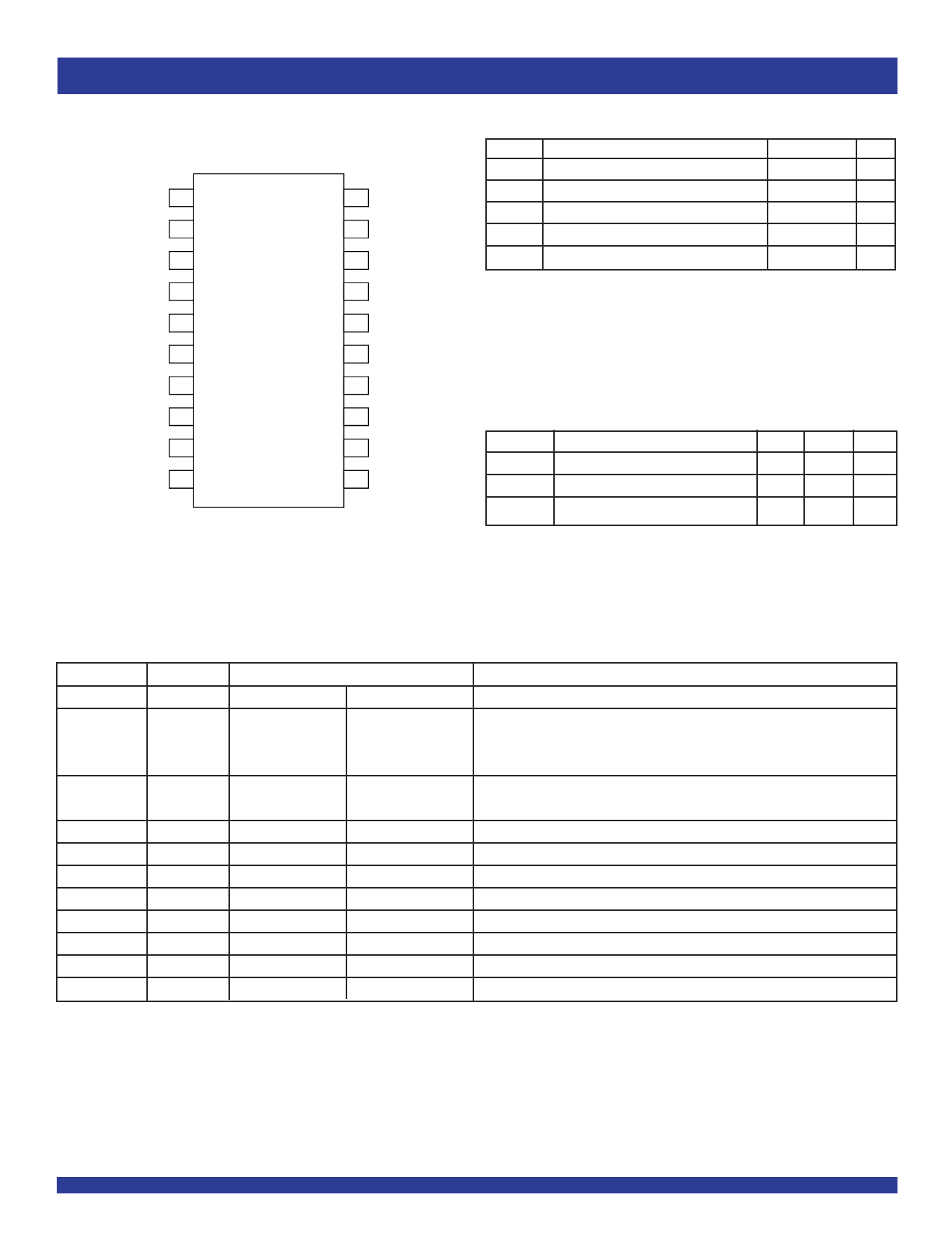
PIN CONFIGURATION
VEE
1
CLK_EN
2
CLK_SEL
3
CLK0
4
NC
5
CLK1
6
NC
7
NC
8
NC
9
VDD
10
20
Q0
19
xQ0
18
VDD
17
Q1
16
xQ1
15
Q2
14
xQ2
13
VDD
12
Q3
11
xQ3
TSSOP
TOP VIEW
COMMERCIAL AND INDUSTRIAL TEMPERATURE RANGES
ABSOLUTE MAXIMUM RATINGS(1)
Symbol
VDD
VI
VO
θJA
Description
Power Supply Voltage
Input Voltage
Output Voltage
Package Thermal Impedance (0 lfpm)
Max
Unit
4.6
V
–0.5 to VDD+0.5 V
–0.5 to VDD+0.5 V
92.6
°C/W
TSTG Storage Temperature
–65 to +150 °C
NOTE:
1. Stresses beyond those listed under ABSOLUTE MAXIMUM RATINGS may cause
permanent damage to the device. These are stress ratings only, and functional
operation of the device at these or any other conditions above those indicated in the
operational sections of this specification is not implied. Exposure to absolute-
maximum-rated conditions for extended periods may affect device reliability.
CAPACITANCE(TA = +25°C, f = 1MHz, VIN = 0V)
Parameter Description
Typ. Max. Unit
CIN
Input Capacitance
—
4
pF
RPULLUP Input Pullup Resistor
51 — K Ω
RPULLDOWN Input Pulldown Resistor
51 — K Ω
PIN DESCRIPTION(1)
Symbol
Number
Type
Description
VEE
1
PWR
Negative Supply Pin
CLK_EN
2
Input
Pullup
Synchronizing Clock Enable. When HIGH, clock outputs follow clock input. When
LOW, Q outputs are forced LOW, xQ outputs are forced HIGH. LVCMOS / LVTTL
interface levels.
CLK_SEL
3
Input
Pulldown
Clock Select Input. When HIGH, selects CLK1 input. When LOW, selects CLK0
input. LVCMOS / LVTTL interface levels.
CLK0
4
Input
Pulldown
LVCMOS / LVTTL Clock Input
CLK1
6
Input
Pulldown
LVCMOS / LVTTL Clock Input
NC
5, 7, 8, 9
Unused
No Connection
VDD
10, 13, 18
Power
Positive Supply Pins
xQ3, Q3
11, 12
Output
Differential Output Pair. LVPECL interface levels.
xQ2 Q2
14, 15
Output
Differential Output Pair. LVPECL interface levels.
xQ1, Q1
16, 17
Output
Differential Output Pair. LVPECL interface levels.
xQ0, Q0
19, 20
Output
Differential Output Pair. LVPECL interface levels.
NOTE:
1. Pullup and Pulldown refer to internal input resistors. See Capacitance table for typical values.
2
Share Link: 