CXB1561Q-Y Ver la hoja de datos (PDF) - Sony Semiconductor
Número de pieza
componentes Descripción
fabricante
CXB1561Q-Y Datasheet PDF : 23 Pages
| |||
CXB1561Q-Y
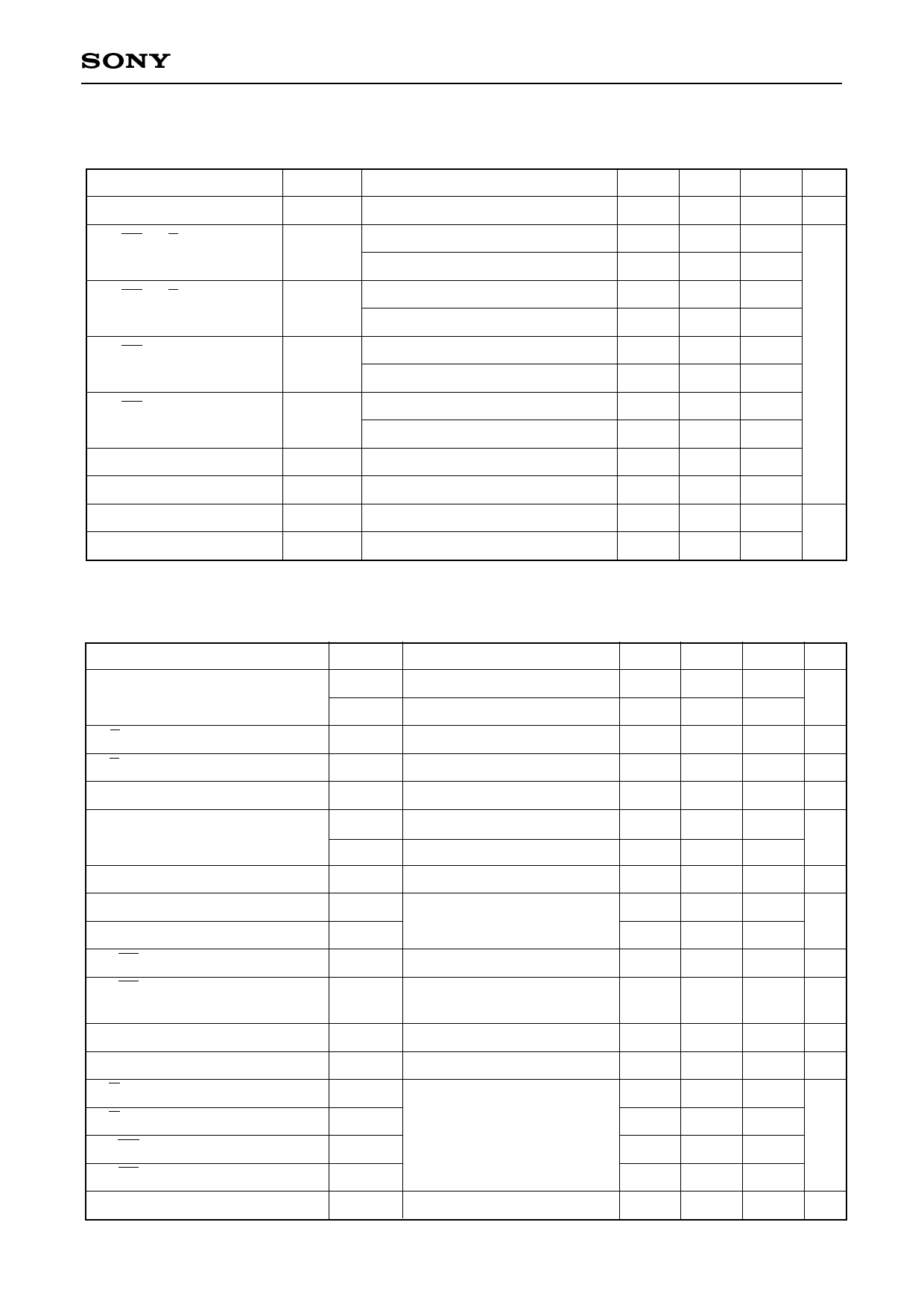
Electrical Characteristics
• DC characteristics
(Vcc = 0V, VEE = –5V ± 10%, Tc = –40 to 85°C)
Item
Symbol
Conditions
Min. Typ. Max. Unit
Supply current
CA/CA, Q/Q
High output voltage
CA/CA, Q/Q
Low output voltage
SD/SD
High output voltage
SD/SD
Low output voltage
IEE
Termination: Rt = 50Ω, VTT = –2V∗1
VOH-Vcc
Termination: Rt = 50Ω, VTT = –2V
VOL-Vcc
Termination: Rt = 50Ω, VTT = –2V∗1
Termination: Rt = 50Ω, VTT = –2V
Termination: Rt = 510Ω, to VEE∗1
VOHa-Vcc
Termination: Rt = 510Ω, to VEE
Termination: Rt = 510Ω, to VEE∗1
VOLa-Vcc
Termination: Rt = 510Ω, to VEE
–157
–1.03
–1.15
–1.81
–1.86
–1.08
–1.20
–1.90
–1.95
–110
–74 mA
–0.88
–0.88
–1.62
–1.60
–0.82
V
–0.83
–1.57
–1.55
S1/S2 High input voltage VIH-Vcc
–1.17
0
S1/S2 Low input voltage VIL-Vcc
–3.00
–1.47
S1/S2 High input current IIH
S1/S2 Low input current IIL
∗1 VEE = –5V, Tc = 0 to 85°C
150
µA
–90
• AC characteristics
(Vcc = 0V, VEE = –5V ± 10%, VTT = –2V, Tc = –40 to 85°C)
Item
Symbol
Conditions
Min. Typ. Max. Unit
Data rate
Da
S2: open low
Db
S2: High
414.72 622.08
155.52 311.04
Mbps
D/D input resistance
RINM
750 1000 1250 Ω
D/D input identification max. voltage VmaxM For single-end input, DC cut-off 1000
mVp-p
Post Amp Gain
GP
Internal signal: 400mV
45
dB
SQ output pulse width
τd1
S2: open low
τd2
S2: High
525 760 1075
ps
1050 1625 2150
SQ output amplitude
VoB
Output, DC cut-off, 50Ω load 480 670 850 mV
SQ rise time
SQ fall time
TrB
50Ω load, 20% to 80%
TfB
200 300 420
ps
200 300 400
SC/SC input resistance
RinL
37.5
50
62.5 Ω
SC/SC input identification max
voltage
VinL
For single-end input, DC cut-off 1000
mVp-p
Limit Amp Gain
GL
Internal signal: 400mV
30
dB
Phase margin for the flip-flop block ∆θ
320 340
deg
Q/Q rise time
TrQ
200 440 650
Q/Q fall time
CA/CA rise time
TfQ
50Ω load, 20% to 80%
TrC
200 410 650
ps
150 245 350
CA/CA fall time
TfC
120 215 350
CA/CA output duty cycle
Du
45
50
55 %
–6–
Share Link: 