DS1977-F5 Ver la hoja de datos (PDF) - Dallas Semiconductor -> Maxim Integrated
Número de pieza
componentes Descripción
fabricante
DS1977-F5 Datasheet PDF : 16 Pages
| |||
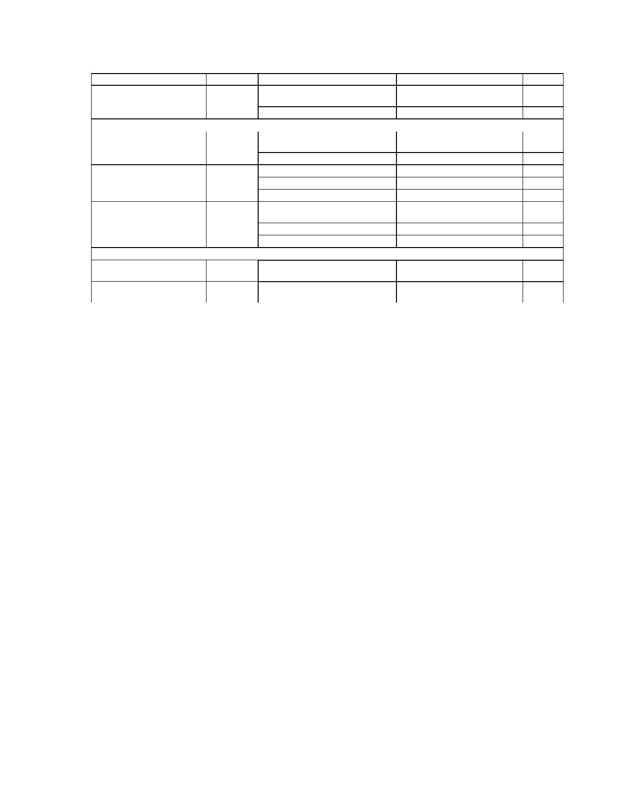
PARAMETER
Write-1 Low Time (Note
11) (system requirement)
IO pin, 1-Wire Read
Read Low Time (Note
12) (system requirement)
Read-0 Low
(data from slave)
Read Sample Time (Note
12)
(system requirement)
VCC Output
IO to VCC Voltage Drop
(Note 13)
Load current
SYMBOL
tW1L
tRL
tSPD
tMSR
∆VIOCC
ILOAD
CONDITIONS
Standard Speed
Overdrive Speed
Standard Speed
Overdrive Speed
Standard Speed, VPUP > 4.5V.
Standard Speed
Overdrive Speed
Standard Speed, VPUP > 4.5V.
Standard Speed
Overdrive Speed
7 mA load current,
VIO = 2.8V
VCC = 2.7 to 5.25V
MIN
5
1
5
1
20
15
2
tRL + δ
tRL + δ
tRL + δ
TYP MAX UNITS
15 - ε
µs
2-ε
µs
15 - δ
µs
2-δ
µs
54
µs
60
µs
6
µs
20
µs
15
µs
2
µs
0.1
V
7
mA
Note 1:
Note 2:
Note 3:
Note 4:
Note 5:
Note 6:
Note 7:
Note 8:
Note 9:
Note 10:
Note 11:
Note 12:
Note 13:
Note 16
This is a requirement that the 1-Wire master has to meet.
Maximum allowable pull-up resistance is a function of the number of 1-Wire devices in the
system and 1-Wire recovery times. The specified value here applies to systems with only
one device and with the minimum 1-Wire recovery times. For more heavily loaded
systems, an active pull-up such as that found in the DS2480B may be required.
VTL, VTH are a function of the internal supply voltage.
Voltage below which, during a falling edge on IO, a logic '0' is detected.
The voltage on IO needs to be less or equal to VILMAX whenever the master drives the line
low.
Voltage above which, during a rising edge on IO, a logic '1' is detected.
After VTH is crossed during a rising edge on IO, the voltage on IO has to drop by VHY to be
detected as logic '0'.
The I-V characteristic is linear for voltages less than 1V.
The earliest recognition of a negative edge is possible at tREH after VTH has been reached
before.
Interval during the negative edge on IO at the beginning of a Presence Detect pulse
between the time at which the voltage is 90% of VPUP and the time at which the voltage is
10% of VPUP.
ε represents the time required for the pull-up circuitry to pull the voltage on IO up from VIL
to VTH.
δ represents the time required for the pull-up circuitry to pull the voltage on IO up from VIL
to the input high threshold of the bus master.
At 7mA load, VCC must not be less than 2.7V, regardless of VIO. If this condition cannot be
met, increase the minimum VPUP to 3.0V or higher.
The strong pull-up must be on when the tDCSA interval elapses. The tDCSA value must be
determined in design as the maximum time required to turn the bypass NCH transistor fully
on.
Page 16
1/31/03
Share Link: 